Modulo LCD TFT da 5,7 pollici con risoluzione 320x240 e schermo touch capacitivo
Modello numero WF57XTIACDNG0
►Dimensione: 5.7 pollici
►Risoluzione : 320 x 240 punti
►Direzione di visione : 12H
►Interfaccia : RGB
►Driver IC:HX8218+HX8615
►Scheda di controllo : Opzione
Luminosità (cd/m²) : 700
►Cornice di fissaggio: No
►Touch Screen : con schermoo touch capacitivo (PCAP)
►Detect Point : 5 Fingers
►O-Film : Opzione
Descrizione
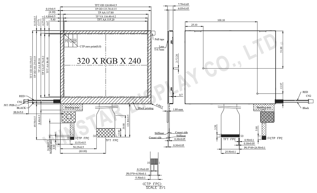
Il WF57XTIACDNG0 è un display LCD TFT da 5,7 pollici con un pannello touch capacitivo proiettato (PCAP). Vanta una risoluzione di 320 x 240 punti e una luminosità di 700 cd/m². Il display TFT è alimentato dal driver IC HX8218+HX8615, che supporta interfacce RGB a 24 bit. La sua alimentazione a tensione varia da 3,2V a 3,4V. Le dimensioni del modulo sono di 126,00 (L) × 101,55 (H) mm, con un'area attiva di 115,2 × 86,40 mm.
Dotato di funzione touch PCAP e del driver IC ILI2130, il WF57XTIACDNG0 supporta interfacce I2C e offre la rilevazione a 5 dita. Offre una direzione di visualizzazione alle 12, inversione scala di grigi alle 6 e un rapporto di aspetto 4:3. La temperatura operativa varia da -20℃ a +70℃, mentre la temperatura di stoccaggio va da -30℃ a +80℃.
Un display touchscreen da 5,7 pollici è versatile e utilizzato in vari settori: Controllo domotico intelligente, Monitoraggio industriale, Diagnostica medica, Intrattenimento in auto, Menù elettronici, Dispositivi portatili intelligenti, Monitoraggio agricolo, Display educativi, Controllo dei segnali stradali, Pagamenti mobili.
DISEGNO
SPECIFICHE TECNICHE
Funzione dei Pin di Interfaccia
LCM PIN Definition
Pin No. | Simbolo | I/O | Funzione |
---|---|---|---|
1 | IF1 | I | Input data format control |
2 | IF2 | I | Input data format control |
3 | POL | O | Polarity Signal connect to VCOM driving circuit. |
4 | RESET | I | Hardware reset. |
5 | SPENA | I | Chip select |
6 | SPCL | I | Serial Clock |
7 | SPDA | I/O | Serial Data |
8 | B0 | I | Blue Data bit (LSB) |
9 | B1 | I | Blue Data bit |
10 | B2 | I | Blue Data bit |
11 | B3 | I | Blue Data bit |
12 | B4 | I | Blue Data bit |
13 | B5 | I | Blue Data bit |
14 | B6 | I | Blue Data bit |
15 | B7 | I | Blue Data bit(MSB) |
16 | G0 | I | Green Data bit(LSB) |
17 | G1 | I | Green Data bit |
18 | G2 | I | Green Data bit |
19 | G3 | I | Green Data bit |
20 | G4 | I | Green Data bit |
21 | G5 | I | Green Data bit |
22 | G6 | I | Green Data bit |
23 | G7 | I | Green Data bit(MSB) |
24 | R0 | I | Red Data bit(LSB) |
25 | R1 | I | Red Data bit |
26 | R2 | I | Red Data bit |
27 | R3 | I | Red Data bit |
28 | R4 | I | Red Data bit |
29 | R5 | I | Red Data bit |
30 | R6 | I | Red Data bit |
31 | R7 | I | Red Data bit(MSB) |
32 | Hsync | I | Horizontal synchronous signal |
33 | Vsync | I | Vertical synchronous signal |
34 | Data CLK | I | Dot data clock |
35 | AVDD | I | 4.5V~5.5V |
36 | AVDD | I | 4.5V~5.5V |
37 | Vcc | I | 3V~3.6V |
38 | Vcc | I | 3V~3.6V |
39 | NPC | O | NTSC/PAL mode Auto detection result H:NTSC/L:PAL |
40 | VGL | I | Gate off power |
41 | VGL | I | Gate off power |
42 | UD | I | Up/Down scan setting. H: Reverse scan / L: Normal scan |
43 | VGH | I | Gate on power |
44 | LRC | I | Shift direction of device internal shift register control. |
45 | GND | I | GROUND |
46 | VCOM | I | VCOM driving input |
47 | VCOM | I | VCOM driving input |
48 | ENB | I | Data enable input. Normally pull low. |
49 | GND | I | GROUND |
50 | GND | I | GROUND |
Backlight PIN Definition
Pin No. | Simbolo | I/O | Funzione |
---|---|---|---|
1 | VLED+ | I | Red, LED_ Anode |
2 | VLED- | I | Black, LED_ Cathode |
PCAP PIN Definition
Pin | Simbolo | Funzione |
---|---|---|
1 | VSS | Ground for analog circuit |
2 | VDDT | Power Supply : +3.3V |
3 | SCL | I2C clock input |
4 | NC | No connect |
5 | SDA | I2C data input and output |
6 | NC | No connect |
7 | /RST | External Reset, Low is active |
8 | NC | No connect |
9 | /INT | External interrupt to the host |
10 | VSS | Ground for analog circuit |
Specifiche generali
Articolo | Dimensioni | Unità |
---|---|---|
Dimensione | 5.7 | pollici |
A matrice di punti | 320 × RGB × 240 (TFT) | dots |
Dimensione del modulo | 126.00(W) × 101.55(H) ×7.79(D) | mm |
Area attiva | 115.2 × 86.40 | mm |
Passo del Dot | 0.12 × 0.36 | mm |
Tipo LCD | TFT, Bianco, Trasmissivo | |
Direzione di visione | 12 o'clock | |
Direzione di inversione della scala dei grigi | 6 o'clock | |
TFT Drive IC | HX8218+HX8615 o equivalente | |
Interfaccia | 24-bit RGB | |
Proporzioni dell’area visiva (ratio) | 4:3 | |
Tipo di backlight | LED, Bianco | |
PCAP FW versione | 0x07.0x00.0x00.0x00.0xA1.0x01.0x57.0x00 | |
PCAP IC | ILI2130 o equivalente | |
PCAP Interfaccia | I2C | |
PCAP Risoluzione | 16384*16384 | |
Con / senza Touch Panel | pannello touch capacitivo (PCAP) | |
Superficie | Bagliore (Glare) |
Valori massimi assoluti
Articolo | Simbolo | Valore Min | Valore tipico | Valore massimo | Unità |
---|---|---|---|---|---|
Temperatura di lavoro | TOP | -20 | - | +70 | ℃ |
Temperatura di stock | TST | -30 | - | +80 | ℃ |
Caratteristiche elettriche
1. Operating conditions:Articolo | Simbolo | Condizione | Valore Min | Valore tipico | Valore massimo | Unità |
---|---|---|---|---|---|---|
Supply Voltage For LCM | VCC | - | 3.2 | 3.3 | 3.4 | V |
AVDD | 4.5 | 5.0 | 5.5 | V | ||
Supply PCAP | VDDT | - | 3.1 | 3.3 | 3.5 | V |
ICTP | - | - | 56 | 84 | mA | |
Input High Volt. | VIH | - | 0.7 VCC | - | VCC | V |
Input Low Volt. | VIL | - | 0 | - | 0.3 VCC | V |
LCD Driving Supply Voltage | VGH *1 | Ta=25℃ | 15 | 16 | 17 | V*3 |
VGL*2 | -6 | -5 | -4 | |||
VcomH | - | 4.5 | - | |||
VcomL | - | -0.5 | - | |||
Supply Current For LCM | IVCC | VCC=3.3V | - | 30 | 45 | mA |
2. LED driving conditions
Parametro | Simbolo | Valore Min | Valore tipico | Valore massimo | Unità | |
---|---|---|---|---|---|---|
|
- | - | 140 | - | mA | |
Consumo di energia | - | 1204 | - | 1470 | mW | |
Tensione LED | VBL+ | 8.6 | 9.5 | 10.5 | V | |
Durata del LED | - | - | 50,000 | - | Hr |