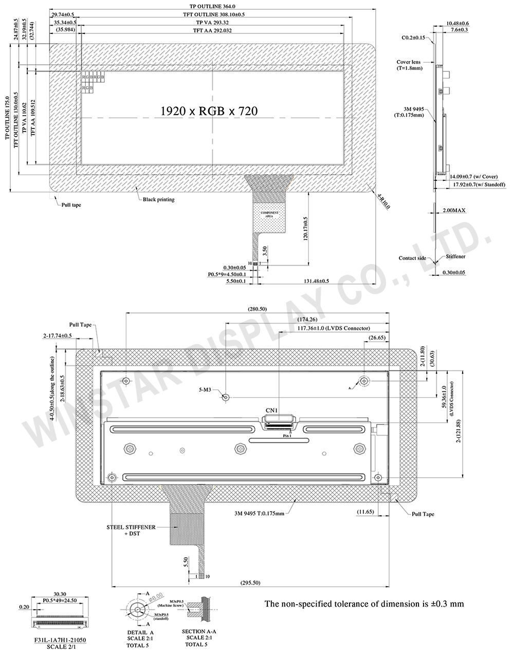
Home Prodotti Schermo TFT Display TFT ad alta luminosità WF123BSWAYLNB0

Display TFT ad alta luminosità da 12.3", 1920x720 con PCAP, LVDS

Modello numero WF123BSWAYLNB0

►Dimensione : 12.3 pollici
►Risoluzione : 1920x720 punti
►Direzione di visione : 85/85/85/85 (IPS)
►Interfaccia : 2ch-LVDS
►Driver IC : HX8298-C01-LT+HX8695-E-LT
►Scheda di controllo: No
►Luminosità(cd/m²): 650
►Cornice di fissaggio: No
►Touch Screen : con pannello touch capacitivo (PCAP)
►Detect Point : 10 Fingers
►Temperatura di funzionamento: -30~+85℃ (Vasta Gamma di Temperature)

DISEGNO

12.3 inch TFT High Brightness Display 1920x720 with PCAP, LVDS Interface - WF123BSWAYLNB0

SPECIFICHE TECNICHE

Funzione dei Pin di Interfaccia

TFT LCD Module

FPC connector is used for electronics interface.
AORORA F31L-1A7H1-21050 , 50PIN

Pin no. Simbolo Funzione
1 GND Ground
2 NC No connector
3 VCC Digital Power
4 VCC Digital Power
5 GND Panel Power
6 GND Panel Power
7 NC No connector
8 NC No connector
9 GND Ground
10 ORXIN0- Odd pixel negative LVDS differential clock input
11 ORXIN0+ Odd pixel positive LVDS differential clock input
12 ORXIN1- Odd pixel negative LVDS differential clock input
13 ORXIN1+ Odd pixel positive LVDS differential clock input
14 ORXIN2- Odd pixel negative LVDS differential clock input
15 ORXIN2+ Odd pixel positive LVDS differential clock input
16 ORXCLKIN- Odd pixel negative LVDS differential clock input
17 ORXCLKIN+ Odd pixel positive LVDS differential clock input
18 ORXIN3- Odd pixel negative LVDS differential clock input
19 ORXIN3+ Odd pixel positive LVDS differential clock input
20 ERXIN0- Even pixel negative LVDS differential clock input
21 ERXIN0+ Even pixel positive LVDS differential clock input
22 ERXIN1- Even pixel negative LVDS differential clock input
23 ERXIN1+ Even pixel positive LVDS differential clock input
24 ERXIN2- Even pixel negative LVDS differential clock input
25 ERXIN2+ Even pixel positive LVDS differential clock input
26 ERXCLKIN- Even pixel negative LVDS differential clock input
27 ERXCLKIN+ Even pixel positive LVDS differential clock input
28 ERXIN3- Even pixel negative LVDS differential clock input
29 ERXIN3+ Even pixel positive LVDS differential clock input
30 GND Ground
31 NC No connector
32 RESETB Global reset pin, active low.
33 STBYB Standby mode, active low.
34 CA3 Output signal to indicate self protection mode, when DE,HS,VS,DCLK, any of these signals is missing, it will become High. If using this pin, CA3 need to pulled low by an resistor,else , let it floating.
35 SCL Serial interface clock input. (User folating)
36 SDA Serial interface data input/output.(User folating)
37 CSB Serial interface chip enable.(User folating)
38 GND Power Ground
39 GND Power Ground
40 NC No connector
41 LEDA LED power (Anode)
42 LEDA LED power (Anode)
43 LEDA LED power (Anode)
44 NC No connector
45 LEDK1 Cathode 1
46 LEDK2 Cathode 2
47 LEDK3 Cathode 3
48 LEDK4 Cathode 4
49 NTC_A NTC_Anode
50 NTC_K NTC_Cathode
 

PCAP PIN Definition

Pin Simbolo Funzione
1 USB_VSS System ground
2 USB_VDD 5V Power supply
3 USB_D+ Data +
4 USB_D- Data -
5 VSS System ground
6 SDA I2C data input and output
7 SCL I2C clock input
8 RST External Reset, Low is active
9 INT External interrupt to the host
10 VDDT 3.3 Power supply

Specifiche generali

Articolo Dimensioni Unità
Dimensione 12.3 pollici
A matrice di punti 1920 RGB (H) × 720(V) pixel
Dimensione del modulo 364.0(H) × 175.0 (V) × 10.48 mm
Area attiva 292.032(H) × 109.512(V) mm
Dimensioni del Dot 0.1521(H) × 0.1521 (V) mm
Tipo LCD TFT, Nero, Trasmissivo
Driver IC HX8298-C01-LT+HX8695-E-LT o equivalente
Direzione di visione 85/85/85/85
Tipo di backlight LED, Bianco
TFT Interfaccia 2ch-LVDS
PCAP IC ILI2511o equivalente
PCAP Interfaccia USB (I2C available)
versione PCAP FW V6.0.0.0.0.0.0.3
Pannello touch con pannello touch capacitivo, PCAP
Superficie Bagliore (Glare)

Valori massimi assoluti

Articolo Simbolo Valore Min Valore tipico Valore massimo Unità
Temperatura di lavoro TOP -30 +85
Temperatura di stock TST -40 +85

Caratteristiche elettriche

Articolo Simbolo Valore Min Valore tipico Valore massimo Unità
Supply Voltage VCC 3 3.3 3.6 V
Input signal voltage ViH VCC *0.7 - VCC V
ViL 0 - VCC *0.3 V
Current of power supply ICC - - 500 mA
Inrush current IRUSH - - 2.0 A
Supply PCAP (USB) USB_VDD 5V 4.75 5.0 5.25 V
I USB_VDD - 90 135 mA
Supply PCAP (I2C) VDDT 3.3 3.15 3.3 3.45 V
IVDDT - 90 135 mA
go top
close