WF123BSWAYLNB0 ist ein 12,3 Zoll TFT-LCD-Modul mit hoher Helligkeit und einer Auflösung von 1920 x 720, ausgestattet mit einem projizierten kapazitiven Touchpanel (PCAP). Dieses Modul unterstützt eine 2-Kanal LVDS (Low-Voltage-Differential-Signaling) Schnittstelle, die für größere TFT LCD-Displays immer populärer wird. Die LVDS-Schnittstelle ist eine ausgezeichnete Lösung aufgrund ihrer hohen Datenübertragungsgeschwindigkeit, niedrigen Spannungsnutzung und verbesserten Rauschunterdrückung. Sie bietet mehrere Vorteile für TFT-Displays, wie eine deutlich geringere Anfälligkeit für EMI (elektromagnetische Interferenzen) und Übersprechprobleme. Sie ermöglicht auch die effektive Übertragung von Daten zu Peripheriegeräten, die eine hohe Bandbreite erfordern, wie hochauflösende Grafiken und schnelle Bildraten, wobei das übertragende Gerät weiter vom Display entfernt sein kann.
Das kapazitive Touchpanel dieses Moduls ist mit dem ILI2511 IC ausgestattet, das über eine USB- oder I2C-Schnittstelle kommunizieren kann und 10 Erkennungspunkte unterstützt.
WF123BSWAYLNB0 verwendet ein IPS-Panel, das den Vorteil eines größeren Betrachtungswinkels bietet: Links: 85°, Rechts: 85°, Oben: 85°, Unten: 85° (typische Werte). Das Panel hat außerdem ein Kontrastverhältnis von 1100:1 (typischer Wert) und eine Helligkeit von 650 Nits (typischer Wert).
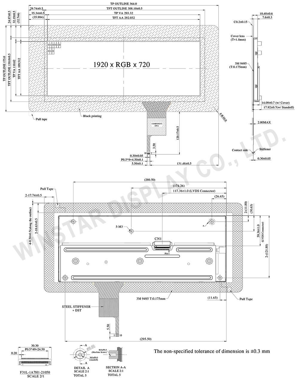
Die Betriebsspannung (VCC) für WF123BSWAYLNB0 liegt im Bereich von 3V bis 3,6V, mit einem typischen Wert von 3,3V. Es funktioniert in einem weiten Temperaturbereich von -30℃ bis +85℃, mit Lagertemperaturen von -40℃ bis +85℃. Wenn Kunden einen weiteren Lagertemperaturbereich von -40℃ bis +90℃ benötigen, können sie unser Modell WF123BSWAYLNBA wählen. Bitte beachten Sie, dass sich die Dicke dieser beiden Module leicht unterscheidet: WF123BSWAYLNB0 hat eine Dicke von 10,48 mm, während WF123BSWAYLNBA eine Dicke von 10,7 mm aufweist.

 - WF123BSWAYLNB0")
 - WF123BSWAYLNB0")


 - WL0F00043000WGAACSA00")


