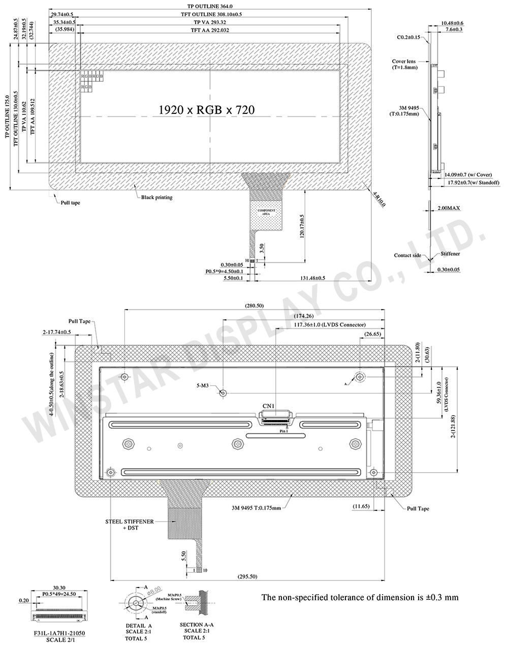
Wysoka jasność wyświetlaczy TFT 12.3 calowy, 1920x720 (PCAP, LVDS)
Numer modelu WF123BSWAYLNB0
►Rozmiar : 12.3 calowy
►Rozdzielczość : 1920x720 punktów
►godzina obserwacji : 85/85/85/85 (IPS)
►Interfejs : 2ch-LVDS
►Kontroler : HX8298-C01-LT+HX8695-E-LT
►płyta kontrolera : brak
►Jasność (cd/m²): 650
►Frame Through Hole : brak
►Panel dotykowy : Pojemnościowy panel dotykowy (PCAP)
►Detect Point : 10 Fingers
►temperatura pracy : -30~+85℃ (TFT o szerokim zakresie temperatur)
Rysunek
Specyfikacja
Funkcja pinów interfejsu
TFT LCD Module
FPC connector is used for electronics interface.
AORORA F31L-1A7H1-21050 , 50PIN
Pin no. | Symbol | Funkcja |
---|---|---|
1 | GND | Ground |
2 | NC | No connector |
3 | VCC | Digital Power |
4 | VCC | Digital Power |
5 | GND | Panel Power |
6 | GND | Panel Power |
7 | NC | No connector |
8 | NC | No connector |
9 | GND | Ground |
10 | ORXIN0- | Odd pixel negative LVDS differential clock input |
11 | ORXIN0+ | Odd pixel positive LVDS differential clock input |
12 | ORXIN1- | Odd pixel negative LVDS differential clock input |
13 | ORXIN1+ | Odd pixel positive LVDS differential clock input |
14 | ORXIN2- | Odd pixel negative LVDS differential clock input |
15 | ORXIN2+ | Odd pixel positive LVDS differential clock input |
16 | ORXCLKIN- | Odd pixel negative LVDS differential clock input |
17 | ORXCLKIN+ | Odd pixel positive LVDS differential clock input |
18 | ORXIN3- | Odd pixel negative LVDS differential clock input |
19 | ORXIN3+ | Odd pixel positive LVDS differential clock input |
20 | ERXIN0- | Even pixel negative LVDS differential clock input |
21 | ERXIN0+ | Even pixel positive LVDS differential clock input |
22 | ERXIN1- | Even pixel negative LVDS differential clock input |
23 | ERXIN1+ | Even pixel positive LVDS differential clock input |
24 | ERXIN2- | Even pixel negative LVDS differential clock input |
25 | ERXIN2+ | Even pixel positive LVDS differential clock input |
26 | ERXCLKIN- | Even pixel negative LVDS differential clock input |
27 | ERXCLKIN+ | Even pixel positive LVDS differential clock input |
28 | ERXIN3- | Even pixel negative LVDS differential clock input |
29 | ERXIN3+ | Even pixel positive LVDS differential clock input |
30 | GND | Ground |
31 | NC | No connector |
32 | RESETB | Global reset pin, active low. |
33 | STBYB | Standby mode, active low. |
34 | CA3 | Output signal to indicate self protection mode, when DE,HS,VS,DCLK, any of these signals is missing, it will become High. If using this pin, CA3 need to pulled low by an resistor,else , let it floating. |
35 | SCL | Serial interface clock input. (User folating) |
36 | SDA | Serial interface data input/output.(User folating) |
37 | CSB | Serial interface chip enable.(User folating) |
38 | GND | Power Ground |
39 | GND | Power Ground |
40 | NC | No connector |
41 | LEDA | LED power (Anode) |
42 | LEDA | LED power (Anode) |
43 | LEDA | LED power (Anode) |
44 | NC | No connector |
45 | LEDK1 | Cathode 1 |
46 | LEDK2 | Cathode 2 |
47 | LEDK3 | Cathode 3 |
48 | LEDK4 | Cathode 4 |
49 | NTC_A | NTC_Anode |
50 | NTC_K | NTC_Cathode |
PCAP PIN Definition
Pin | Symbol | Funkcja |
---|---|---|
1 | USB_VSS | System ground |
2 | USB_VDD 5V | Power supply |
3 | USB_D+ | Data + |
4 | USB_D- | Data - |
5 | VSS | System ground |
6 | SDA | I2C data input and output |
7 | SCL | I2C clock input |
8 | RST | External Reset, Low is active |
9 | INT | External interrupt to the host |
10 | VDDT 3.3 | Power supply |
Ogólna specyfikacja
Rzecz | Wymiar | Jednostka |
---|---|---|
Rozmiar | 12.3 | calowy |
Matryca punktowa | 1920 RGB (H) × 720(V) | pixel |
Wymiary modułu | 364.0(H) × 175.0 (V) × 10.48 | mm |
Obszar aktywny | 292.032(H) × 109.512(V) | mm |
Raster pomiędzy pikselami | 0.1521(H) × 0.1521 (V) | mm |
Rodzaj LCD | TFT, czarny, Transmisyjny | |
Kontroler | HX8298-C01-LT+HX8695-E-LT albo odpowiednik | |
Kąt obserwacji | 85/85/85/85 | |
Rodzaj podświetlenia | LED, biały | |
TFT Interfejs | 2ch-LVDS | |
PCAP IC | ILI2511 albo odpowiednik | |
PCAP Interfejs | USB (I2C available) | |
PCAP FW Version | V6.0.0.0.0.0.0.3 | |
Panel dotykowy | PCAP,pojemnościowy panel dotykowy | |
Powierzchnia | Glare |
Bezwzględne oceny maksymalne
Rzecz | Symbol | Minimalna wartość | Typowa wartość | Maksymalna wartość | Jednostka |
---|---|---|---|---|---|
Temperatura pracy | TOP | -30 | - | +85 | ℃ |
Temperatura przechowywania | TST | -40 | - | +85 | ℃ |
Parametry elektryczne
Rzecz | Symbol | Minimalna wartość | Typowa wartość | Maksymalna wartość | Jednostka |
---|---|---|---|---|---|
Supply Voltage | VCC | 3 | 3.3 | 3.6 | V |
Input signal voltage | ViH | VCC *0.7 | - | VCC | V |
ViL | 0 | - | VCC *0.3 | V | |
Current of power supply | ICC | - | - | 500 | mA |
Inrush current | IRUSH | - | - | 2.0 | A |
Supply PCAP (USB) | USB_VDD 5V | 4.75 | 5.0 | 5.25 | V |
I USB_VDD | - | 90 | 135 | mA | |
Supply PCAP (I2C) | VDDT 3.3 | 3.15 | 3.3 | 3.45 | V |
IVDDT | - | 90 | 135 | mA |