


3.12" дюймовый графический COF OLED с платой
Артикул. WEN025664B
►Тип: Графический
►Тип монтажа контроллера: COF+PCB+Frame
►Диагональ: 3.12 дюйма
►Разрешение: 256 x 64 точек
►Встроенный контроллер SSD1322
►3V Power supply
►1/64 duty
►Интерфейс: 6800, 8080, SPI
►Цвет дисплея: Белый / Желтый / Небесно голубой / Зеленый
►Инверсия
Описание
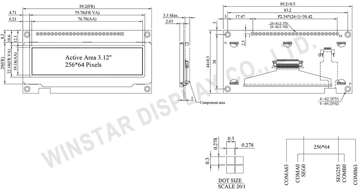
WEN025664B это COF OLED модуль на печатной платой; диагональ модуля 3.12" с разрешением 256х64 точек. WEN025664B сделан на базе контроллера IC SSD1322 c поддержкой интерфейсов: параллельного 6800/8080 и 3-х/4-х жильного SPI интерфейса. Напряжение питания логики 3.3 V, а рабочий цикл (duty cycle) составляет 1/64. Значение тока при засвете 50% площади индикатора составляет 150 mA @3Vdd (типичное значение). Размер печатной платы дисплея составляет 89.2 × 44.0 mm и имеет монтажные отверстия для наиболее удобного крепления на устройстве.
WEN025664B COG OLED модуль может работать при температурах от -40℃ до + 80℃; а температура хранения - от -40℃ до +85℃.
Кроме того, OLED-панели одинакового размера предлагают различные альтернативы:- Серия WEX025664B без металлической рамки и печатной платы.
- Серия WEX025664B-CTP без металлической рамки, печатной платы и с сенсорным экраном CTP.
- Серия WEN025664B-CTP с металлической рамкой, печатной платой и сенсорным экраном CTP.
Чертеж
Data source ref: WEN025664BWAP3N0000
Технические характеристики
Функции контроллера контактного интерфейса
| Pin Number |
Символы | I/O | Описание | ||||||||||
|---|---|---|---|---|---|---|---|---|---|---|---|---|---|
| 1 | VSS | P | Ground. | ||||||||||
| 2 | VDD | P | Power Supply for Core Logic Circuit Power supply pin for core logic operation. A capacitor is required to connect between this pin and VSS |
||||||||||
| 3 | N.C. | P | Reserved Pin The N.C. pin between function pins are reserved for compatible and flexible design. |
||||||||||
| 4 | D/C# | I | Data/Command Control This pin is Data/Command control pin connecting to the MCU. When the pin is pulled HIGH, the content at D[7:0] will be interpreted as data. When the pin is pulled LOW, the content at D[7:0] will be interpreted as command. |
||||||||||
| 5 | R/W# (WR#) |
I | Read/Write Select or Write This pin is MCU interface input. When interfacing to a 68XX-series microprocessor, this pin will be used as Read/Write (R/W#) selection input. Pull this pin to “High” for read mode and pull it to “Low” for write mode. When 80XX interface mode is selected, this pin will be the Write (WR#) input. Data write operation is initiated when this pin is pulled low and the CS# is pulled low. When serial mode is selected, this pin must be connected to VSS. |
||||||||||
| 6 | E/RD# | I | Read/Write Enable or Read This pin is MCU interface input. When interfacing to a 68XX-series microprocessor, this pin will be used as the Enable (E) signal. Read/write operation is initiated when this pin is pulled high and the CS# is pulled low. When connecting to an 80XX-microprocessor, this pin receives the Read (RD#) signal. Data read operation is initiated when this pin is pulled low and CS# is pulled low. When serial mode is selected, this pin must be connected to VSS. |
||||||||||
| 7~14 | DB0 | I/O | Host Data Input/Output Bus These pins are 8-bit bi-directional data bus to be connected to the microprocessor’s data bus. When serial mode is selected, DB1 will be the serial data input SDIN and DB0 will be the serial clock input SCLK. |
||||||||||
| DB1 | |||||||||||||
| DB2 | |||||||||||||
| DB3 | |||||||||||||
| DB4 | |||||||||||||
| DB5 | |||||||||||||
| DB6 | |||||||||||||
| DB7 | |||||||||||||
| 15 | NC | P | Reserved Pin The N.C. pin between function pins are reserved for compatible and flexible design. |
||||||||||
| 16 | RES# | I | This pin is reset signal input. When the pin is pulled LOW, initialization of the chip is executed. Keep this pin pull HIGH during normal operation. |
||||||||||
| 17 | CS# | I | Data/Command Control This pin is the chip select input connecting to the MCU. The chip is enabled for MCU communication only when CS# is pulled LOW. |
||||||||||
18 |
NC | P | Reserved Pin The N.C. pin between function pins are reserved for compatible and flexible design. |
||||||||||
| 19 | BS1 | I | Communicating Protocol Select These pins are MCU interface selection input. See the following table:
(1) 0 is connected to VSS (2) 1 is connected to VDD |
||||||||||
| 20 | BS0 | ||||||||||||
| 21~24 | NC | P | Reserved Pin The N.C. pin between function pins are reserved for compatible and flexible design. |
Механические характеристики
| Наименование | Измерения | Единица |
|---|---|---|
| Разрешение | 256 x 64 Dots | - |
| Габариты | 89.2 × 44.0 × 3.3 Max. | mm |
| Активная область | 76.78 × 19.18 | mm |
| Размер пикселя | 0.278 × 0.278 | mm |
| Шаг пикселя | 0.3 × 0.3 | mm |
| Матрица | Пассивная | |
| Цвет дисплея | монохромные | |
| Рабочий цикл | 1/64 Duty | |
| Шкала серого | 4 bits | |
| IC | SSD1322 (COF) | |
| Интерфейс | 6800, 8080, SPI | |
| Диагональ | 3.12 дюйма | |
Абсолютные максимальные значения
| Параметр | Символы | Минимальный | Максимальный | Единица |
|---|---|---|---|---|
| Supply Voltage for Display | VDD | -0.3 | 4 | V |
| Диапазон рабочих температур | TOP | -40 | 80 | °C |
| Температура хранения | TSTG | -40 | 85 | °C |
Электронные характеристики
| Наименование | Символы | Кондиция | Минимальный | Типичный | Максимальный | Единица |
|---|---|---|---|---|---|---|
| Напряжение питания дисплея | VDD | - | 2.8 | 3.0 | 3.3 | V |
| Вход высокого уровня | VIH | - | 0.8×VDD | - | VDD | V |
| Вход низкого уровня | VIL | - | 0 | - | 0.2×VDD | V |
| Выход высокого уровня | VOH | - | 0.9×VDD | - | VDD | V |
| Выход низкого уровня | VOL | - | 0 | - | 0.1×VDD | V |
| 50% Check Board operating Current | IDD | VCC =3V | - | 150 | 300 | mA |
Search keyword: 256x64 oled, oled 256x64, 3.12 oled, 3.12" oled, 3.12 дюйма oled, oled 3.12, oled 3.12"
