


N° de modèle WEN025664B
►Type: Graphique
►Structure: COF+PCB+Frame
►Dimension: 3.12"
►Matrice de points 256 x 64
►Contrôleur intégré SSD1322
►Alimentation 3V
►1/64 duty
►Interface: 6800, 8080, SPI
►Couleur d'affichage: Blanc / Jaune / Bleu ciel / Vert
►Support Grayscale
Description
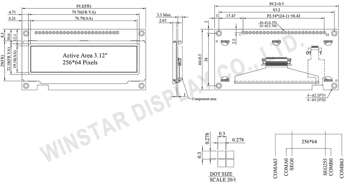
Le modèle WEN025664B est un OLED graphique COF de 3,12 pouces, avec une diagonale et une résolution de 256x64 points. Ce module OLED est intégré au circuit intégré SSD1322 et prend en charge les interfaces 8 bits 6800/8080 et 3/4 lignes SPI. Il a des dimensions extérieures de 89,2 × 44,0 mm, avec une zone active de 76,78 × 19,18 mm. Il prend également en charge une échelle de gris de 4 bits, avec une tension logique d'alimentation de 3V. Le courant de l'écran avec 50 % de la carte de contrôle est de 150 mA à 3,0 V VDD (valeur typique), avec un cycle de travail de 1/64.
Le module a une carte de circuit imprimé (PCB) intégrée, permettant aux clients d'utiliser des connexions par fil sans avoir besoin d'un développement de PCB supplémentaire pour leurs applications. De plus, le circuit VCC intégré sur le PCB simplifie l'utilisation par le client. Cette carte de circuit imprimé (PCB), équipée de quatre trous de montage, offre une méthode facile aux clients pour fixer les modules dans leurs applications. Ce module OLED convient aux applications domotiques, aux dispositifs médicaux, à la commande industrielle, etc.
Le modèle WEN025664B peut fonctionner à des températures allant de -40 °C à +80 °C, avec des températures de stockage allant de -40 °C à +85 °C. Le module OLED présente un rapport de contraste élevé de 10 000:1, ce qui se traduit par une amélioration de la qualité de l'image, des détails plus nets et une meilleure lisibilité, en particulier dans des environnements faiblement éclairés.
De plus, les panneaux OLED avec les mêmes dimensions offrent diverses alternatives :- Série WEX025664B sans cadre métallique et PCB.
- Série WEX025664B-CTP sans cadre métallique, PCB, avec un écran tactile CTP.
- Série WEN025664B-CTP avec cadre métallique, PCB et écran tactile CTP.
DESSIN
Data source ref: WEN025664BWAP3N0000
SPÉCIFICATIONS
Fonction PIN sur l'interface
| Pin Number |
Symbole | I/O | Description | ||||||||||
|---|---|---|---|---|---|---|---|---|---|---|---|---|---|
| 1 | VSS | P | Ground. | ||||||||||
| 2 | VDD | P | Power Supply for Core Logic Circuit Power supply pin for core logic operation. A capacitor is required to connect between this pin and VSS |
||||||||||
| 3 | N.C. | P | Reserved Pin The N.C. pin between function pins are reserved for compatible and flexible design. |
||||||||||
| 4 | D/C# | I | Data/Command Control This pin is Data/Command control pin connecting to the MCU. When the pin is pulled HIGH, the content at D[7:0] will be interpreted as data. When the pin is pulled LOW, the content at D[7:0] will be interpreted as command. |
||||||||||
| 5 | R/W# (WR#) |
I | Read/Write Select or Write This pin is MCU interface input. When interfacing to a 68XX-series microprocessor, this pin will be used as Read/Write (R/W#) selection input. Pull this pin to “High” for read mode and pull it to “Low” for write mode. When 80XX interface mode is selected, this pin will be the Write (WR#) input. Data write operation is initiated when this pin is pulled low and the CS# is pulled low. When serial mode is selected, this pin must be connected to VSS. |
||||||||||
| 6 | E/RD# | I | Read/Write Enable or Read This pin is MCU interface input. When interfacing to a 68XX-series microprocessor, this pin will be used as the Enable (E) signal. Read/write operation is initiated when this pin is pulled high and the CS# is pulled low. When connecting to an 80XX-microprocessor, this pin receives the Read (RD#) signal. Data read operation is initiated when this pin is pulled low and CS# is pulled low. When serial mode is selected, this pin must be connected to VSS. |
||||||||||
| 7~14 | DB0 | I/O | Host Data Input/Output Bus These pins are 8-bit bi-directional data bus to be connected to the microprocessor’s data bus. When serial mode is selected, DB1 will be the serial data input SDIN and DB0 will be the serial clock input SCLK. |
||||||||||
| DB1 | |||||||||||||
| DB2 | |||||||||||||
| DB3 | |||||||||||||
| DB4 | |||||||||||||
| DB5 | |||||||||||||
| DB6 | |||||||||||||
| DB7 | |||||||||||||
| 15 | NC | P | Reserved Pin The N.C. pin between function pins are reserved for compatible and flexible design. |
||||||||||
| 16 | RES# | I | This pin is reset signal input. When the pin is pulled LOW, initialization of the chip is executed. Keep this pin pull HIGH during normal operation. |
||||||||||
| 17 | CS# | I | Data/Command Control This pin is the chip select input connecting to the MCU. The chip is enabled for MCU communication only when CS# is pulled LOW. |
||||||||||
18 |
NC | P | Reserved Pin The N.C. pin between function pins are reserved for compatible and flexible design. |
||||||||||
| 19 | BS1 | I | Communicating Protocol Select These pins are MCU interface selection input. See the following table:
(1) 0 is connected to VSS (2) 1 is connected to VDD |
||||||||||
| 20 | BS0 | ||||||||||||
| 21~24 | NC | P | Reserved Pin The N.C. pin between function pins are reserved for compatible and flexible design. |
Données mécaniques
| Article | Dimension | Unité |
|---|---|---|
| Matrice de points | 256 x 64 Dots | - |
| Dimensions du module | 89.2 × 44.0 × 3.3 Max. | mm |
| Zone active | 76.78 × 19.18 | mm |
| Taille des points | 0.278 × 0.278 | mm |
| Pas des points | 0.3 × 0.3 | mm |
| Mode d'affichage | Matrice passive | |
| Couleur d'affichage | Monochrome | |
| Drive Duty | 1/64 Duty | |
| Gray Scale | 4 bits | |
| IC | SSD1322 (COF) | |
| Interface | 6800, 8080, SPI | |
| Diagonale | 3.12 pouces | |
Valeurs nominales maximales absolues
| Parameter | Symbole | Valeur min | Valeur max | Unité |
|---|---|---|---|---|
| Supply Voltage for Display | VDD | -0.3 | 4 | V |
| Température de fonctionnement | TOP | -40 | 80 | °C |
| Température de stockage | TSTG | -40 | 85 | °C |
Caractéristiques électroniques
| Article | Symbole | État | Valeur min | Valeur type | Valeur max | Unité |
|---|---|---|---|---|---|---|
| Supply Voltage for Logic | VDD | - | 2.8 | 3.0 | 3.3 | V |
| High Level Input | VIH | - | 0.8×VDD | - | VDD | V |
| Low Level Input | VIL | - | 0 | - | 0.2×VDD | V |
| High Level Output | VOH | - | 0.9×VDD | - | VDD | V |
| Low Level Output | VOL | - | 0 | - | 0.1×VDD | V |
| 50% Check Board operating Current | IDD | VCC =3V | - | 150 | 300 | mA |
Search keyword: 256x64 oled, oled 256x64, 3.12 oled, 3.12" oled, 3.12 pouces oled, oled 3.12, oled 3.12 pouces
