


Écran OLED 3,12 pouces COF - Résolution 256x64
N° de modèle WEX025664B
►Type: Graphique
►Structure: COF
►Dimension: 3.12"
►Matrice de points 256 x 64
►IC:SSD1322
►Alimentation 3V
►1/64 duty
►Interface: 6800, 8080, SPI
►Couleur d'affichage: Blanc / Jaune / Bleu ciel / Vert
►Support d’échelle grise
Description
Le modèle WEX025664B est un écran graphique OLED COF de 3,12 pouces avec une résolution de 256x64 points. Cet écran OLED de 3,12 pouces est équipé d'un circuit intégré de pilote SSD1322, prenant en charge les interfaces 8 bits 6800/8080 et SPI 3/4 lignes. Il a des dimensions extérieures de 88 x 27,8 mm, avec une zone active de 76,778 x 19,178 mm. L'écran prend en charge 4 bits de niveaux de gris, et sa tension logique est de 2,5 V (valeur typique) avec un cycle de service de 1/64. Le module peut fonctionner à des températures de -40°C à +80°C, et sa température de stockage est de -40°C à +85°C.
Le module OLED offre un contraste élevé de 10 000:1, permettant des couleurs plus vibrantes et fidèles à la réalité, des noirs plus profonds et des blancs plus lumineux. Cela se traduit par une amélioration de la qualité d'image, des détails plus nets et une meilleure lisibilité, en particulier dans des environnements peu éclairés. De plus, le contraste élevé contribue à une expérience visuelle plus immersive.
Le module OLED convient à diverses applications telles que les dispositifs mur/mètre, les applications résidentielles, les systèmes POS, les systèmes Cloud/IoT, les instruments portables, les dispositifs de technologie intelligente, les systèmes énergétiques, les applications automobiles, les systèmes de communication et les instruments médicaux. Les clients peuvent mettre à niveau leurs applications actuelles des affichages STN traditionnels vers des affichages OLED, car le module offre une très large gamme de formats de pixels pour les solutions OLED.
De plus, les panneaux OLED avec les mêmes dimensions offrent une variété d'alternatives :- Série WEX025664B-CTP sans cadre métallique, PCB, et avec un écran tactile CTP.
- Série WEN025664B avec un cadre métallique et PCB.
- Série WEN025664B-CTP avec un cadre métallique, PCB, et un écran tactile CTP.
DESSIN
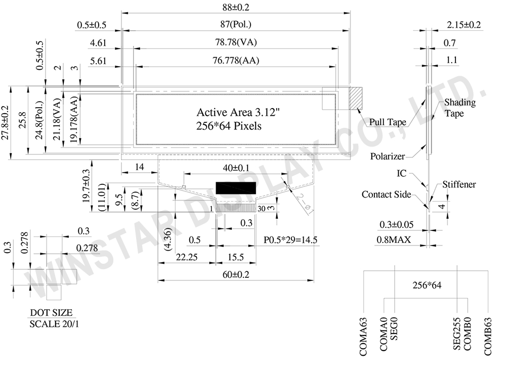
Data source ref: WEX025664BWPP3N00000
SPÉCIFICATIONS
Fonction PIN sur l'interface
| Pin Number | Symbole | I/O | Description | ||||||||||
|---|---|---|---|---|---|---|---|---|---|---|---|---|---|
| 1 | N.C. (GND) | P | Ground | ||||||||||
| 2 | VSS | P | Ground. | ||||||||||
| 3 | VCC | P | Power supply for panel driving voltage. This is also the most positive power voltage supply pin. |
||||||||||
| 4 | VCOMH | P | COM signal deselected voltage level. A capacitor should be connected between this pin and VSS. |
||||||||||
| 5 | VLSS | P | Analog system ground pin. | ||||||||||
| 6~13 | D7~D0 | I/O | Host Data Input/Output Bus These pins are 8-bit bi-directional data bus to be connected to the microprocessor’s data bus. When serial mode is selected, D1 will be the serial data input SDIN and D0 will be the serial clock input SCLK. |
||||||||||
| 14 | E/RD# | I | Read/Write Enable or Read This pin is MCU interface input. When interfacing to a 68XX-series microprocessor, this pin will be used as the Enable (E) signal. Read/write operation is initiated when this pin is pulled high and the CS# is pulled low. When connecting to an 80XX-microprocessor, this pin receives the Read (RD#) signal. Data read operation is initiated when this pin is pulled low and CS# is pulled low. When serial mode is selected, this pin must be connected to VSS. |
||||||||||
| 15 | R/W# | I | Read/Write Select or Write This pin is MCU interface input. When interfacing to a 68XX-series microprocessor, this pin will be used as Read/Write (R/W#) selection input. Pull this pin to “High” for read mode and pull it to “Low” for write mode. When 80XX interface mode is selected, this pin will be the Write (WR#) input. Data write operation is initiated when this pin is pulled low and the CS# is pulled low. When serial mode is selected, this pin must be connected to VSS. |
||||||||||
| 16 | BS0 | I | Communicating Protocol Select These pins are MCU interface selection input. See the following table:
(1) 0 is connected to VSS (2) 1 is connected to VDDIO |
||||||||||
| 17 | BS1 | ||||||||||||
| 18 | D/C# | I | Data/Command Control This pin is Data/Command control pin connecting to the MCU. When the pin is pulled HIGH, the content at D[7:0] will be interpreted as data. When the pin is pulled LOW, the content at D[7:0] will be interpreted as command. |
||||||||||
| 19 | CS# | I | Data/Command Control This pin is the chip select input connecting to the MCU. The chip is enabled for MCU communication only when CS# is pulled LOW. |
||||||||||
| 20 | RES# | I | This pin is reset signal input. When the pin is pulled LOW, initialization of the chip is executed. Keep this pin pull HIGH during normal operation. |
||||||||||
| 21 | FR | O | This pin is No Connection pins. Nothing should be connected to this pin. This pin should be left open individually. | ||||||||||
| 22 | IREF | I | Current Reference for Brightness Adjustment This pin is segment current reference pin. A resistor should be connected between this pin and VSS. Set the current lower than 10uA. |
||||||||||
| 23 | N.C. | - | Reserved Pin The N.C. pin between function pins are reserved for compatible and flexible design. |
||||||||||
| 24 | VDDIO | P | Power Supply for I/O Pin It should be matched with the MCU interface voltage level. |
||||||||||
| 25 | VDD | P | Power Supply for Core Logic Circuit Power supply pin for core logic operation. A capacitor is required to connect between this pin and VSS |
||||||||||
| 26 | VCI | P | Power Supply for Operation VCI must always be equal to or higher than VDD and VDDIO. |
||||||||||
| 27 | VSL | P | Voltage Output Low Level for SEG Signal This is segment voltage reference pin. When external VSL is not used, this pin should be left open. When external VSL is used, this pin should connect with resistor and diode to ground. |
||||||||||
| 28 | VLSS | P | Ground of Analog Circuit These are the analog ground pins. They should be connected to VSS externally. |
||||||||||
| 29 | VCC | P | Power Supply for OLED Panel These are the most positive voltage supply pin of the chip. They must be connected to external source. |
||||||||||
| 30 | N.C. (GND) | P | Ground |
Données mécaniques
| Article | Dimension | Unité |
|---|---|---|
| Matrice de points | 256 x 64 Dots | - |
| Dimensions du module | 88.0 × 27.8 × 2.15 | mm |
| Zone active | 76.778×19.178 | mm |
| Taille des points | 0.278×0.278 | mm |
| Pas des points | 0.3×0.3 | mm |
| Mode d'affichage | Matrice passive | |
| Couleur d'affichage | Monochrome | |
| Drive Duty | 1/64 Duty | |
| Gray Scale | 4 bits | |
| IC | SSD1322 (COF) | |
| Interface | 6800, 8080, SPI | |
| Diagonale | 3.12 pouces | |
Valeurs nominales maximales absolues
| Parameter | Symbole | Valeur min | Valeur max | Unité |
|---|---|---|---|---|
| Supply Voltage for Operation | VCI | -0.3 | 4 | V |
| Supply Voltage for Logic | VDD | -0.5 | 2.75 | V |
| Supply Voltage for I/O Pins | VDDIO | -0.5 | VCI | V |
| Supply Voltage for Display | VCC | -0.5 | 20 | V |
| Température de fonctionnement | TOP | -40 | 80 | °C |
| Température de stockage | TSTG | -40 | 85 | °C |
Caractéristiques électroniques
| Article | Symbole | État | Valeur min | Valeur type | Valeur max | Unité |
|---|---|---|---|---|---|---|
| Supply Voltage for Logic | VDD | - | 2.4 | 2.5 | 2.6 | V |
| Power Supply for I/O pins | VDDIO | - | 1.65 | 3.0 | VCI | V |
| Low voltage power supply | VCI | - | 2.4 | 3.0 | 3.5 | V |
| Supply Voltage for Display | VCC | - | 11.5 | 14.5 | 15 | V |
| High Level Input | VIH | - | 0.8×VDDIO | - | VDDIO | V |
| Low Level Input | VIL | - | 0 | - | 0.2×VDDIO | V |
| High Level Output | VOH | - | 0.9×VDDIO | - | VDDIO | V |
| Low Level Output | VOL | - | 0 | - | 0.1×VDDIO | V |
| 50% Check Board operating Current | ICC | VCC =12V | - | 24 | 32 | mA |
| VCC =14.5V | - | 32 | 42.5 | mA |
Search keyword: 256x64 oled, oled 256x64, 3.12 oled, 3.12" oled, 3.12 pouces oled, oled 3.12, oled 3.12 pouces
