


2.8 дюймовый 256x64 COF OLED с поддержкой градации серого, с печатной платой и рамкой
Артикул. WEN025664A
►Тип: Графический
►Тип монтажа контроллера: COF+FR+PCB
►Диагональ: 2.8 дюйма
►Разрешение: 256×64 точек
►IC:SSD1322
►3V power supply
►1/64 duty cycle
►Интерфейс: 6800, 8080, SPI
►Цвет дисплея: Белый / Желтый
►Инверсия
Описание
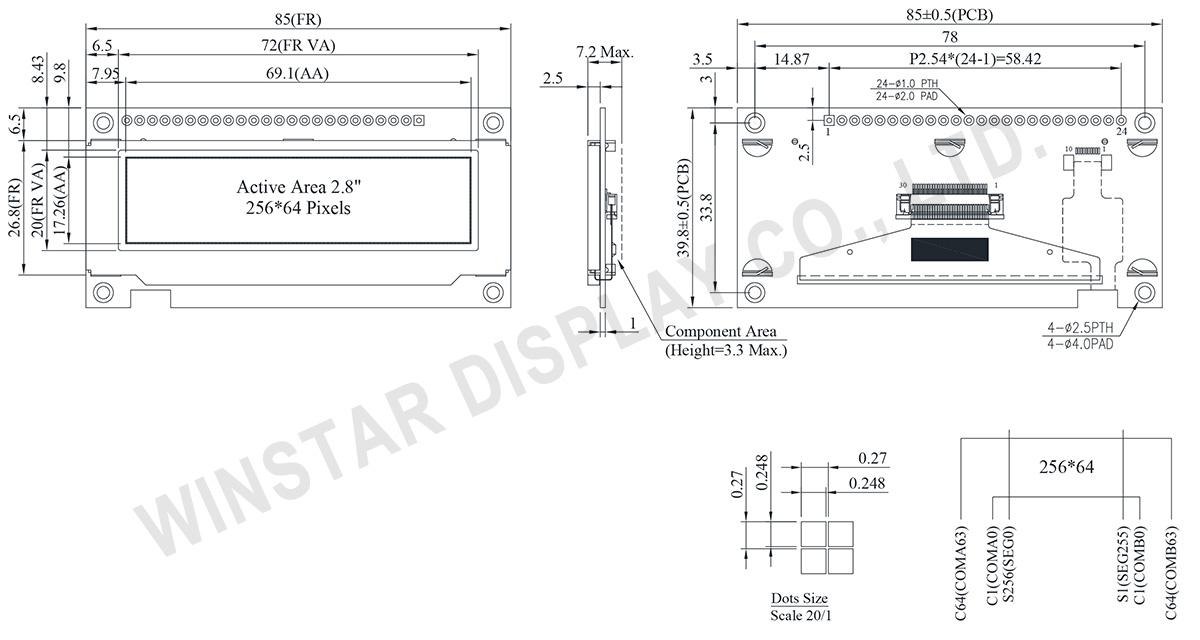
WEN025664A серия представляет собой 2.8-дюймовый монохромный графический COF OLED-дисплей с разрешением 256x64 точек. Он оснащен IC SSD1322 и поддерживает несколько интерфейсов, включая 6800/8080 8-битные и 3/4-проводные SPI-интерфейсы. Габаритные размеры модуля WEN025664A составляют 85.0 × 39.8 мм, а активная область - 69.1 × 17.26 мм.
OLED-серия WEN025664A работает от источника питания 3 В с методом управления 1/64. Она поддерживает градации серого и имеет высокое соотношение контрастности 10 000:1. Модуль способен функционировать в диапазоне температур от -40°C до +80°C, с диапазоном температур хранения от -40°C до +83°C.
С металлической рамой, печатной платой и четырьмя отверстиями для винтов, WEN025664A обеспечивает легкость установки для клиентов. OLED-серия, оснащенная печатной платой, легко соединяется с приложениями с использованием проводов, что исключает необходимость разработки дополнительных печатных плат для клиентов. Интеграция настроек интерфейса и цепей VDD повышает удобство использования. Кроме того, четыре отверстия для винтов на печатной плате упрощают процесс установки на приложение.
Серия WEN025664A также предлагает вариант с тем же OLED-панелью, но с сенсорным панелью. Пожалуйста, выберите серию WEN025664A-CTP для опции с сенсорной панелью.
Чертеж
Data source ref: WEN025664ALAP3N00000
Технические характеристики
Функции контроллера контактного интерфейса
| Pin Number | Символ | I/O | Описание | ||||||||||
|---|---|---|---|---|---|---|---|---|---|---|---|---|---|
| 1 | VSS | P | Ground. | ||||||||||
| 2 | VDD | P | Power Supply for Core Logic Circuit Power supply pin for core logic operation. A capacitor is required to connect between this pin and VSS |
||||||||||
| 3 | N.C. | P | Reserved Pin The N.C. pin between function pins are reserved for compatible and flexible design. |
||||||||||
| 4 | D/C# | I | Data/Command Control This pin is Data/Command control pin connecting to the MCU. When the pin is pulled HIGH, the content at D[7:0] will be interpreted as data. When the pin is pulled LOW, the content at D[7:0] will be interpreted as command. |
||||||||||
| 5 | R/W# (WR#) |
I | Read/Write Select or Write This pin is MCU interface input. When interfacing to a 68XX-series microprocessor, this pin will be used as Read/Write (R/W#) selection input. Pull this pin to “High” for read mode and pull it to “Low” for write mode. When 80XX interface mode is selected, this pin will be the Write (WR#) input. Data write operation is initiated when this pin is pulled low and the CS# is pulled low. When serial mode is selected, this pin must be connected to VSS. |
||||||||||
| 6 | E/RD# | I | Read/Write Enable or Read This pin is MCU interface input. When interfacing to a 68XX-series microprocessor, this pin will be used as the Enable (E) signal. Read/write operation is initiated when this pin is pulled high and the CS# is pulled low. When connecting to an 80XX-microprocessor, this pin receives the Read (RD#) signal. Data read operation is initiated when this pin is pulled low and CS# is pulled low. When serial mode is selected, this pin must be connected to VSS. |
||||||||||
| 7~14 | DB0 | I/O | Host Data Input/Output Bus These pins are 8-bit bi-directional data bus to be connected to the microprocessor’s data bus. When serial mode is selected, DB1 will be the serial data input SDIN and DB0 will be the serial clock input SCLK. |
||||||||||
| DB1 | |||||||||||||
| DB2 | |||||||||||||
| DB3 | |||||||||||||
| DB4 | |||||||||||||
| DB5 | |||||||||||||
| DB6 | |||||||||||||
| DB7 | |||||||||||||
| 15 | NC | P | Reserved Pin The N.C. pin between function pins are reserved for compatible and flexible design. |
||||||||||
| 16 | RES# | I | This pin is reset signal input. When the pin is pulled LOW, initialization of the chip is executed. Keep this pin pull HIGH during normal operation. |
||||||||||
| 17 | CS# | I | Data/Command Control This pin is the chip select input connecting to the MCU. The chip is enabled for MCU communication only when CS# is pulled LOW. |
||||||||||
| 18 | NC | P | Reserved Pin The N.C. pin between function pins are reserved for compatible and flexible design. |
||||||||||
| 19 | BS1 | I | Communicating Protocol Select These pins are MCU interface selection input. See the following table:
(1) 0 is connected to VSS (2) 1 is connected to VDD |
||||||||||
| 20 | BS0 | ||||||||||||
| 21~24 | NC | P | Reserved Pin The N.C. pin between function pins are reserved for compatible and flexible design. |
Механические характеристики
| Наименование | Измерения | Единица |
|---|---|---|
| Разрешение | 256 x 64 точек | - |
| Габариты | 85.0 × 39.8 × 7.2 Max. | mm |
| Активная область | 69.1 × 17.26 | mm |
| Размер пикселя | 0.248 × 0.248 | mm |
| Шаг пикселя | 0.27 × 0.27 | mm |
| Матрица | Пассивная | |
| Цвет дисплея | монохромные | |
| Рабочий цикл | 1/64 Duty | |
| OLED IC | SSD1322 (COF) | |
| OLED Интерфейс | 6800, 8080, SPI | |
| Диагональ | 2.8 дюйма | |
Абсолютные максимальные значения
| Параметр | Символы | Минимальный | Максимальный | Единица |
|---|---|---|---|---|
| Supply Voltage for Display | VDD | -0.3 | 4 | V |
| Диапазон рабочих температур | TOP | -40 | +80 | °C |
| Температура хранения | TSTG | -40 | +85 | °C |
Электронные характеристики
DC Электронные характеристики
| Наименование | Символы | Кондиция | Минимальный | Типичный | Максимальный | Единица |
|---|---|---|---|---|---|---|
| Напряжение питания логических схем | VDD | - | 2.8 | 3.0 | 3.3 | V |
| Вход высокого уровня | VIH | - | 0.8×VDD | - | VDD | V |
| Вход низкого уровня | VIL | - | 0 | - | 0.2×VDD | V |
| Выход высокого уровня | VOH | - | 0.9×VDD | - | VDD | V |
| Выход низкого уровня | VOL | - | 0 | - | 0.1×VDD | V |
| 50% Check Board operating Current | IDD | VDD =3V | - | 125 | 250 | mA |
Search keyword: 256x64 oled, oled 256x64, 2.8 oled, 2.8" oled, 2.8 дюйма oled, oled 2.8"
