


1.5 inch 128x128 COG Graphic OLED Display
Model No. WEO128128H
►Type: Graphic
►Structure: COG
►Size:1.5 inch
►128 x 128 Dot Matrix
►IC:CH1120
►3V Power supply
►1/128 Duty
►Interface: 8080,SPI,I2C
►Display Color: White / Yellow
►Support Grayscale
Description
WEO128128H is a 1.5-inch COG Graphic OLED display featuring 4-bits grayscale function; made of resolution of 128x128 pixels. This module is built-in with CH1120 IC; it supports 8080, SPI, I2C interface, 1/128 driving duty, the supply voltage for Logic is 3V (VDD), and the supply voltage for display is 12V. The current with 50% checkerboard display is 20mA @ VCC 12V for white and 14.5V for yellow.
WEO128128H is a COG structure OLED display module that is lightweight, low power, and very thin. It is suitable for smart home applications, Cloud/IoT systems, handheld instruments, intelligent technology devices, energy systems, automotive, communication systems, medical instruments, etc. WEO128128H OLED module can be operated at temperatures from -40℃ to +80℃; its storage temperatures range from -40℃ to +85℃.
DRAWING
Data source ref:WEO128128HLAP3N00000
SPECIFICATIONS
Interface Pin Function
| No. | Symbol | Function | |||||||||||||||
|---|---|---|---|---|---|---|---|---|---|---|---|---|---|---|---|---|---|
| 1 | ESD_GND | This pin should be connected to GND. | |||||||||||||||
| 2 | VPP | This is the most positive voltage supply pin of the chip. It should be supplied externally. |
|||||||||||||||
| 3 | VCOMH | This is a pin for the voltage output high level for common signals. A capacitor should be connected between this pin and GND. |
|||||||||||||||
| 4 | VDD | Power supply for logic | |||||||||||||||
| 5 | NC | No connection | |||||||||||||||
| 6 | IM1 | These are the MPU interface mode select pins.
|
|||||||||||||||
| 7 | IM2 | ||||||||||||||||
| 8 | VSS | Ground for logic and analog. This pin should be connected to GND externally. | |||||||||||||||
| 9 | IREF | This is a segment current reference pin. A resistor should be connected between this pin and GND. |
|||||||||||||||
| 10 | CSB | This pin is the chip select input. When CSB = “L”, then the chip select becomes active, and data/command I/O is enabled. When in I2C interface, this pin is not used, so it must be connected to “L”. |
|||||||||||||||
| 11 | RESB | This is a reset signal input pin. When RESB is set to “L”, the settings are initialized. The reset operation is performed by the RESB signal level. This pin internal pull high. | |||||||||||||||
| 12 | A0 | This is the Data/Command control pin that determines whether the data bits are data or a command. A0 = “H”: the inputs at D0 to D7 are treated as display data A0 = “L”: the inputs at D0 to D7 are transferred to the command registers. In I2C interface, this pin serves as SA0 to distinguish the different address of OLED driver. When in 3-wire interface, this pin is not used, so it must be connected to “L”. |
|||||||||||||||
| 13 | WRB | This is a MPU interface input pin. When connected to an 8080 MPU, this is active LOW. This pin connects to the 8080 MPU WR signal. The signals on the data bus are latched at the rising edge of the WR signal When in 3-wire.4-wire & I2C interface, this pin is not used, so it must be connected to “L”. |
|||||||||||||||
| 14 | RDB | This is a MPU interface input pin. When connected to an 8080 series MPU, it is active LOW. This pin is connected to the RD signal of the 8080 series MPU, and the data bus is in an output status when this signal is “L”. When in 3-wire.4-wire & I2C interface, this pin is not used, so it must be connected to “L”. |
|||||||||||||||
| 15 | D0 | This is an 8-bit bi-directional data bus that connects to an 8-bit or 16-bit standard MPU data bus. When the serial interface(SPI) and I2C is selected, then D0 serves as the serial clock input pin (SCL) and D1 serves as the serial data input pin (SI). At this time, D2 to D7 are set to high impedance. D7~D2 is recommended to connect the VDD or GND. It is also allowed to leave D7~D2 unconnected. |
|||||||||||||||
| 16 | D1 | ||||||||||||||||
| 17 | D2 | ||||||||||||||||
| 18 | D3 | ||||||||||||||||
| 19 | D4 | ||||||||||||||||
| 20 | D5 | ||||||||||||||||
| 21 | D6 | ||||||||||||||||
| 22 | D7 | ||||||||||||||||
| 23 | VPP | This is the most positive voltage supply pin of the chip It should be supplied externally. |
|||||||||||||||
| 24 | ESD_GND | This pin should be connected to GND. |
Mechanical Data
| Item | Dimension | Unit |
|---|---|---|
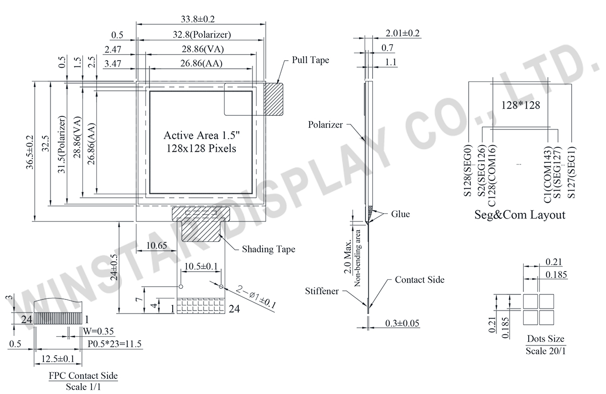
| Dot Matrix | 128 × 128 | dots |
| Module dimension | 33.80 x 36.50 x 2.01 | mm |
| Active Area | 26.86 x 26.86 | mm |
| Pixel Size | 0.185 x 0.185 | mm |
| Pixel Pitch | 0.210 x 0.210 | mm |
| Display Mode | Passive Matrix | |
| Display Color | Monochrome | |
| Drive Duty | 1/128 Duty | |
| Gray Scale | 4 bits | |
| IC | CH1120 | |
| Interface | 8080,SPI,I2C | |
| Size | 1.5 inch | |
Absolute Maximum Ratings
| Parameter | Symbol | Min | Max | Unit |
|---|---|---|---|---|
| Supply Voltage for Logic | VDD | -0.3 | 3.5 | V |
| Supply Voltage for Display | VPP | -0.3 | 15.0 | V |
| Operating Temperature | TOP | -40 | +80 | °C |
| Storage Temperature | TSTG | -40 | +85 | °C |
Electronical Characteristics
| Item | Symbol | Condition | Min | Typ | Max | Unit |
|---|---|---|---|---|---|---|
| Supply Voltage for Logic | VDD | - | 1.65 | 3.0 | 3.3 | V |
| Supply Voltage for Display | VPP | - | 8.0 | 14.5 | 15.0 | V |
| High Level Input | VIH | - | 0.8×VDD | - | VDD | V |
| Low Level Input | VIL | - | GND | - | 0.2×VDD | V |
| High Level Output | VOH | - | 0.8×VDD | - | VDD | V |
| Low Level Output | VOL | - | GND | - | 0.1×VDD | V |
| Display 50% Pixel on | IPP | VPP=14.5V | - | 20 | 30 | mA |
Search keyword: 128x128 oled, oled 128x128,1.5 oled, 1.5" oled, 1.5inch oled, oled 1.5, oled 1.5"
