


1.5 ", 128x128 Графические OLED дисплей
Артикул. WEO128128H
►Тип: Графический
►Тип монтажа контроллера: COG
►Диагональ: 1.5 дюйма
►Разрешение: 128 x 128 точек
►IC:CH1120
►3V Power supply
►1/128 duty
►Интерфейс:8080,SPI,I2C
►Цвет дисплея: Белый / Желтый
►Инверсия
Описание
WEO128128H – 1.5'' дюймовый графический COG OLED модуль с разрешением 128x128 и поддержкой 16-ти оттенков серого (4 бит). Данный дисплей сделан на базе контроллера IC CH1120 c поддержкой I2C и SPI интерфейса. Напряжение питания модуля - 12V(типичное значение), напряжение питания логики дисплея – 3 VDD, а рабочий цикл 1/128. Значение тока при засвете 50% площади индикатора составляет 20mA@ 12V для белого OLED, и 14.5V для желтого OLED. WEO128128H может работать при температурах от –40°С до +80°С; а температура хранения от –40°С до +85°С.
WEO128128H OLED создан по технологии «chip–on–glass», что позволило сделать его очень тонким! Этот легкий и тонкий индикатор идеально подойдет для таких применений как: медицинские приборы, системы «умного дома», терминалы оплаты, Облачные/IoT системы, умные устройства, автомобилестроение, коммуникационные системы, измерительные приборы, датчики и т.д.
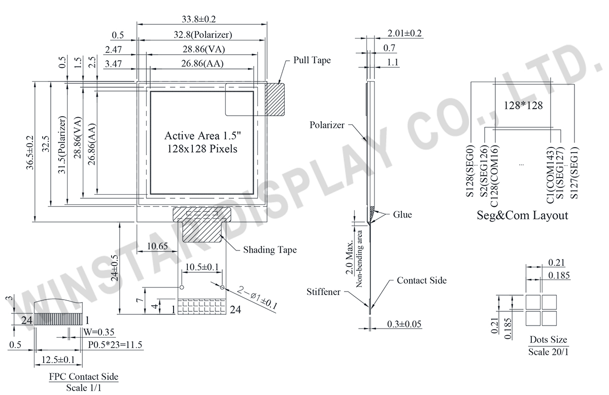
Чертеж
Data source ref:WEO128128HLAP3N00000
Технические характеристики
Функции контроллера контактного интерфейса
| No. | Символы | Описание | |||||||||||||||
|---|---|---|---|---|---|---|---|---|---|---|---|---|---|---|---|---|---|
| 1 | ESD_GND | This pin should be connected to GND. | |||||||||||||||
| 2 | VPP | This is the most positive voltage supply pin of the chip. It should be supplied externally. |
|||||||||||||||
| 3 | VCOMH | This is a pin for the voltage output high level for common signals. A capacitor should be connected between this pin and GND. |
|||||||||||||||
| 4 | VDD | Power supply for logic | |||||||||||||||
| 5 | NC | No connection | |||||||||||||||
| 6 | IM1 | These are the MPU interface mode select pins.
|
|||||||||||||||
| 7 | IM2 | ||||||||||||||||
| 8 | VSS | Ground for logic and analog. This pin should be connected to GND externally. | |||||||||||||||
| 9 | IREF | This is a segment current reference pin. A resistor should be connected between this pin and GND. |
|||||||||||||||
| 10 | CSB | This pin is the chip select input. When CSB = “L”, then the chip select becomes active, and data/command I/O is enabled. When in I2C interface, this pin is not used, so it must be connected to “L”. |
|||||||||||||||
| 11 | RESB | This is a reset signal input pin. When RESB is set to “L”, the settings are initialized. The reset operation is performed by the RESB signal level. This pin internal pull high. | |||||||||||||||
| 12 | A0 | This is the Data/Command control pin that determines whether the data bits are data or a command. A0 = “H”: the inputs at D0 to D7 are treated as display data A0 = “L”: the inputs at D0 to D7 are transferred to the command registers. In I2C interface, this pin serves as SA0 to distinguish the different address of OLED driver. When in 3-wire interface, this pin is not used, so it must be connected to “L”. |
|||||||||||||||
| 13 | WRB | This is a MPU interface input pin. When connected to an 8080 MPU, this is active LOW. This pin connects to the 8080 MPU WR signal. The signals on the data bus are latched at the rising edge of the WR signal When in 3-wire.4-wire & I2C interface, this pin is not used, so it must be connected to “L”. |
|||||||||||||||
| 14 | RDB | This is a MPU interface input pin. When connected to an 8080 series MPU, it is active LOW. This pin is connected to the RD signal of the 8080 series MPU, and the data bus is in an output status when this signal is “L”. When in 3-wire.4-wire & I2C interface, this pin is not used, so it must be connected to “L”. |
|||||||||||||||
| 15 | D0 | This is an 8-bit bi-directional data bus that connects to an 8-bit or 16-bit standard MPU data bus. When the serial interface(SPI) and I2C is selected, then D0 serves as the serial clock input pin (SCL) and D1 serves as the serial data input pin (SI). At this time, D2 to D7 are set to high impedance. D7~D2 is recommended to connect the VDD or GND. It is also allowed to leave D7~D2 unconnected. |
|||||||||||||||
| 16 | D1 | ||||||||||||||||
| 17 | D2 | ||||||||||||||||
| 18 | D3 | ||||||||||||||||
| 19 | D4 | ||||||||||||||||
| 20 | D5 | ||||||||||||||||
| 21 | D6 | ||||||||||||||||
| 22 | D7 | ||||||||||||||||
| 23 | VPP | This is the most positive voltage supply pin of the chip It should be supplied externally. |
|||||||||||||||
| 24 | ESD_GND | This pin should be connected to GND. |
Механические характеристики
| Наименование | Измерения | Единица |
|---|---|---|
| Разрешение | 128 × 128 | dots |
| Габариты | 33.80 x 36.50 x 2.01 | mm |
| Активная область | 26.86 x 26.86 | mm |
| Размер пикселя | 0.185 x 0.185 | mm |
| Шаг пикселя | 0.210 x 0.210 | mm |
| Матрица | Пассивная матрица | |
| Цвет дисплея | монохромные | |
| Рабочий цикл | 1/128 Duty | |
| Серая шкала | 4 bits | |
| IC | CH1120 | |
| Интерфейс | 8080,SPI,I2C | |
| Диагональ | 1.5 inch | |
Абсолютные максимальные значения
| Параметр | Символы | Минимальный | Максимальный | Единица |
|---|---|---|---|---|
| Напряжение питания логических схем | VDD | -0.3 | 3.5 | V |
| Напряжение питания дисплея | VPP | -0.3 | 15.0 | V |
| Диапазон рабочих температур | TOP | -40 | +80 | °C |
| Температура хранения | TSTG | -40 | +85 | °C |
Электронные характеристики
| Наименование | Символы | Кондиция | Минимальный | Типичный | Максимальный | Единица |
|---|---|---|---|---|---|---|
| Напряжение питания логических схем | VDD | - | 1.65 | 3.0 | 3.3 | V |
| Напряжение питания Display | VPP | - | 8.0 | 14.5 | 15.0 | V |
| Высокое входное напряжение | VIH | - | 0.8×VDD | - | VDD | V |
| Низкое входное напряжение | VIL | - | GND | - | 0.2×VDD | V |
| д высокого уровня | VOH | - | 0.8×VDD | - | VDD | V |
| Выход низкого уровня | VOL | - | GND | - | 0.1×VDD | V |
| Display 50% Pixel on | IPP | VPP=14.5V | - | 20 | 30 | mA |
Search keyword: 128x128 oled, oled 128x128,1.5 oled, 1.5" oled, 1.5дюйма oled, oled 1.5, oled 1.5"
