


我們重視您的隱私
通過點擊「允許所有 Cookie」,代表您同意在您的設備上存儲 Cookie 以增強網站瀏覽體驗、分析網站使用情況並協助我們的行銷和網站效能優化工作。您可以在我們的隱私權政策中找到有關於此的更多資訊。


| 項目 | 規格 | 單位 |
|---|---|---|
| 尺寸(對角線) | 7 | 吋 |
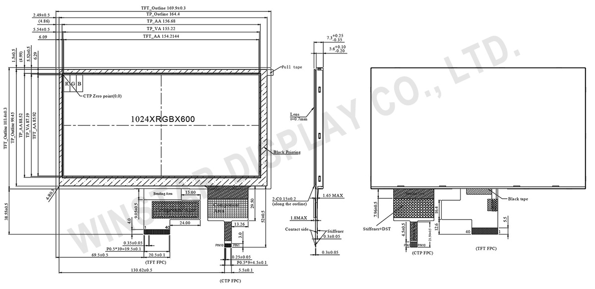
| 點陣(解析度) | 1024 × RGB × 600(TFT) | dots |
| 模組尺寸 | 169.9(W) × 103.4(H) × 7.3(D) | mm |
| 有效區域 | 154.2144 × 85.92 | mm |
| 點間距 | 0.1506 × 0.1432 | mm |
| LCD類型 | IPS TFT 全透 | |
| 視角 | 85/85/85/85 | |
| TFT 介面 | LVDS | |
| 長寬比 | 16:9 | |
| TFT 驅動 IC | ST5021 + ST5651或相容IC | |
| 背光類型 | LED, 白光 | |
| PCTP IC | ILI2130 或相容IC | |
| PCAP 介面 | I2C | |
| PCAP FW 版本 | 0x07.0x00.0x00.0x00.0x65.0x90.0x00.0x01 | |
| 觸控面板 | 投射電容式觸控面板 | |
| 表面 | 亮面 | |
| 項目 | 符號 | 最小值 | 典型值 | 最大值 | 單位 |
|---|---|---|---|---|---|
| 工作溫度 | TOP | -20 | - | +70 | ℃ |
| 儲存溫度 | TST | -30 | - | +80 | ℃ |
| 項目 | 符號 | 標準值 | 單位 | ||
|---|---|---|---|---|---|
| 最小值 | 典型值 | 最大值 | |||
| 電源電壓 | VDD | 3.0 | 3.3 | 3.6 | V |
| PCAP電源電壓 | VDDT | 3.0 | 3.3 | 3.6 | V |
| ICTP | - | 65 | 98 | mA | |
| 類比電源電壓 | AVDD | 8.9 | 9.0 | 9.1 | V |
| TFT VGH 電壓 | VGH | 17 | 18 | 19 | V |
| TFT VGL 電壓 | VGL | -6.5 | -6.0 | -5.5 | V |
| TFT Vcom 電壓 | Vcom | 3.0 | 3.15 | 3.3 | V |
| 驅動電流 | IDD | - | 14 | 21 | mA |
| 電源電流 | IAVDD | - | 25 | - | mA |
| TFT IVGH 電流 | IVGH | - | 1 | - | mA |
| TFT IVGL 電流 | IVGL | - | 1 | - | mA |
| TFT IVCOM 電流 | IVCOM | - | 1 | - | mA |
| Pin No. | 符號 | I/O | 功能說明 |
|---|---|---|---|
| 1 | VCOM | P | Common Voltage |
| 2 | VDD | P | Digital circuit |
| 3 | VDD | P | Digital circuit |
| 4 | NC | --- | No connection |
| 5 | RESET | I | Global reset pin |
| 6 | STBYB | I | Standby mode, Normally pulled high STBYB = “1”, normal operation STBYB = “0”, timing controller, source driver will turn off, all output are High-Z |
| 7 | GND | P | Ground |
| 8 | RXIN0- | I | Negative LVDS differential data input |
| 9 | RXIN0+ | I | Positive LVDS differential data input |
| 10 | GND | P | Ground |
| 11 | RXIN1- | I | Negative LVDS differential data input |
| 12 | RXIN1+ | I | Positive LVDS differential data input |
| 13 | GND | P | Ground |
| 14 | RXIN2- | I | Negative LVDS differential data input |
| 15 | RXIN2+ | I | Positive LVDS differential data input |
| 16 | GND | P | Ground |
| 17 | RXCLKIN- | I | Negative LVDS differential clock input |
| 18 | RXCLKIN+ | I | Positive LVDS differential clock input |
| 19 | GND | P | Ground |
| 20 | RXIN3- | I | Negative LVDS differential data input |
| 21 | RXIN3+ | I | Positive LVDS differential data input |
| 22 | GND | P | Ground |
| 23 | NC | --- | No connection |
| 24 | NC | --- | No connection |
| 25 | GND | P | Ground |
| 26 | NC | --- | No connection |
| 27 | NC | --- | No connection |
| 28 | SELB | I | 6bit/8bit mode select H:6bit / L:8bit |
| 29 | AVDD | P | Power for Analog Circuit |
| 30 | GND | P | Ground |
| 31 | LED- | P | LED Cathode |
| 32 | LED- | P | LED Cathode |
| 33 | L/R | I | Horizontal inversion |
| 34 | U/D | I | Vertical inversion |
| 35 | VGL | P | Negative power for TFT |
| 36 | NC | --- | No connection |
| 37 | NC | --- | No connection |
| 38 | VGH | P | Positive power for TFT |
| 39 | LED+ | P | LED Anode |
| 40 | LED+ | P | LED Anode |
I:input ,O:output,P:power
| Pin | 符號 | 功能說明 |
|---|---|---|
| 1 | VSS | Ground for analog circuit |
| 2 | VDDT | Power Supply : +3.3V |
| 3 | SCL | I2C clock input |
| 4 | NC | No connect |
| 5 | SDA | I2C data input and output |
| 6 | NC | No connect |
| 7 | /RST | External Reset, Low is active |
| 8 | NC | No connect |
| 9 | /INT | External interrupt to the host |
| 10 | VSS | Ground for analog circuit |

通過點擊「允許所有 Cookie」,代表您同意在您的設備上存儲 Cookie 以增強網站瀏覽體驗、分析網站使用情況並協助我們的行銷和網站效能優化工作。您可以在我們的隱私權政策中找到有關於此的更多資訊。