
我們重視您的隱私
通過點擊「允許所有 Cookie」,代表您同意在您的設備上存儲 Cookie 以增強網站瀏覽體驗、分析網站使用情況並協助我們的行銷和網站效能優化工作。您可以在我們的隱私權政策中找到有關於此的更多資訊。


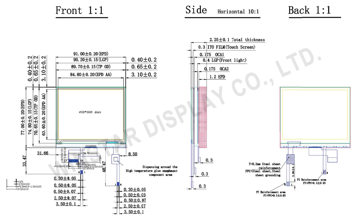
型號 WAA0420A2ADB5NXXX000
►尺寸: 4.2吋
►解析度: 400x300 dots
►介面: SPI
►觸控面板: 電容式觸控面板
►顯示器可以刷新黑白電子紙顯示。
►前光 : 有
WAA0420A2ADB5NXXX000 是一款 4.2 吋電子紙顯示模組(EPD),具備前光面板與電容式觸控功能。此顯示器支援 1-bit 黑白影像顯示,解析度為 400×300 像素。採用 TFT 背板驅動電泳層,內建多種功能電路,包括 Gate Driver、Source Driver、MCU 介面、定時控制器、振盪器、DC-DC 轉換器、SRAM、LUT 及 VCOM 產生器。
此模組專為超低功耗及高可視環境設計,適用於多種商業與工業應用場景中無紙化顯示的需求。
這款 4.2 吋電子紙顯示模組不僅適用於 電子貨架標籤(ESL) 系統,亦適合多種低功耗、高清晰度的顯示應用,包括:
| 參數 | 規格 | 單位 |
|---|---|---|
| 尺寸 | 4.2 | 吋 |
| 解析度 | 400(H)×300(V) | 像素 |
| 有效區域 | 84.8(H)×63.6(V) | mm |
| 像素間距 | 0.212×0.212 | mm |
| 像素配置 | Rectangle | |
| 外型尺寸 | 91(H) × 77 (V) × 2.02(D) | mm |
| 模組重量 | 16.1±0.3 | g |
| 參數 | 符號 | 額定值 | 單位 |
|---|---|---|---|
| 邏輯供電電壓 | VCI | -0.5 to +6.0 | V |
| 邏輯輸入電壓 | VIN | -0.5 to VCI +0.5 | V |
| 邏輯輸出電壓 | VOUT | -0.5 to VCI +0.5 | V |
| 工作溫度範圍 | TOPR | 0 to +50 | ºC |
| 儲存溫度範圍 | TSTG | -25 to+70 | ºC |
| 最佳儲存溫度 | TSTGo | 23±2 | ºC |
| 最佳儲存濕度 | HSTGo | 55±10 | %RH |
| No. | 符號 | I/O | 功能說明 |
|---|---|---|---|
| 1 | NC | Do not connect with other NC pins | |
| 2 | GDR | O | N-Channel MOSFET Gate Drive Control |
| 3 | RESE | I | Current sense input for control loop. |
| 4 | NC | NC | Do not connect with other NC pins |
| 5 | VSH2 | C | Positive source driving voltage (Red) |
| 6 | TSCL | O | I2C interface to digital temperature sensor Clock pin |
| 7 | TSDA | I/O | I2C interface to digital temperature sensor Data pin |
| 8 | BS1 | I | Bus Inteface selection pin |
| 9 | BUSY | O | Busy state output pin |
| 10 | RES# | I | Reset signal input. Active Low |
| 11 | D/C# | I | Data / Command control pin |
| 12 | CS# | I | Chip select input pin |
| 13 | SCL | I | Serial Clock pin (SPI) |
| 14 | SDA | I/O | Serial Data pin (SPI) |
| 15 | VDDIO | P | Power Suupply for interface logic pins. It should be connected with VCI |
| 16 | VCI | P | Power Supply for the chip |
| 17 | VSS | P | Ground |
| 18 | VDD | C | Core logic power pin VDD can be regulated internally from VCI. A capacitor should be connected between VDD and VSS |
| 19 | VPP | P | FOR TEST |
| 20 | VSH1 | C | Positive Source driving voltage |
| 21 | VGH | C | Power Supply pin for Positive Gate driving voltage and VSH1 |
| 22 | VSL | C | Negative Source driving voltage |
| 23 | VGL | C | Power Supply pin for Negative Gate driving voltage VCOM and VSL |
| 24 | VCOM | C | VCOM driving voltage |
Note: I: Input, O: Output, P: Power, D: Dummy, S: Shorted line, M: Mark, PI: Power input, PO: Power output, I/O: Input / Output, PS: Power Setting, C: Capacitor pin.

通過點擊「允許所有 Cookie」,代表您同意在您的設備上存儲 Cookie 以增強網站瀏覽體驗、分析網站使用情況並協助我們的行銷和網站效能優化工作。您可以在我們的隱私權政策中找到有關於此的更多資訊。