

 - WAA0290A2ADA8NXXX000")
 - WL0F00035000XGAABSA00")
我们重视您的隐私
通过点击「允许所有 Cookie」,代表您同意在您的设备上存储 Cookie 以增强网站浏览体验、分析网站使用情况并协助我们的营销和网站效能优化工作。您可以在我们的隐私权政策中找到有关于此的更多信息。


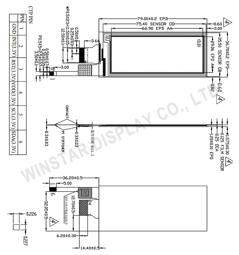
WAA0290A2ABA8NXXX000 是一款 2.9 寸电子纸显示器 (EPD),配备电容触控面板。该显示器能够显示黑白图像,并具备完整的 1 位显示能力。2.9 寸的有效显示区域包含 296x128 像素。此模块使用 TFT 阵列来驱动电子墨水显示,并整合了包括门驱动器、源驱动器、MCU 接口、定时控制器、振荡器、DC-DC 转换器、SRAM、LUT 和 VCOM 控制等集成电路。此模块可用于便携式电子设备,如电子货架标签 (ESL) 系统。
| 参数 | 规格 | 单位 |
|---|---|---|
| 尺寸 | 2.9 | 寸 |
| 分辨率 | 296(H)×128(V) | 像素 |
| 有效区域 | 29.056×66.896 | mm |
| 像素间距 | 0.227×0.226 | mm |
| 像素配置 | Rectangle | |
| 外型尺寸 | 36.7(H) × 79.0 (V) × 1.575(D) | mm |
| 模块重量 | 8.31±0.5 | g |
| 参数 | 符号 | 额定值 | 单位 |
|---|---|---|---|
| 逻辑供电电压 | VCI | -0.5 to +4.0 | V |
| 逻辑输入电压 | VIN | -0.5 to VCI +0.5 | V |
| 逻辑输出电压 | VOUT | -0.5 to VCI +0.5 | V |
| 工作温度范围 | TOPR | 0 to +50 | ºC |
| 储存温度范围 | TSTG | -25 to+70 | ºC |
| 最佳储存温度 | TSTGo | 23±2 | ºC |
| 最佳储存湿度 | HSTGo | 55±10 | %RH |
| No. | 符号 | I/O | 功能说明 |
|---|---|---|---|
| 1 | NC | Do not connect with other NC pins | |
| 2 | GDR | O | N-Channel MOSFET Gate Drive Control |
| 3 | RESE | P | Current sense input for control loop. |
| 4 | NC | NC | Do not connect with other NC pins |
| 5 | VSH2 | C | Positive source driving voltage (Red) |
| 6 | TSCL | O | I2C interface to digital temperature sensor Clock pin |
| 7 | TSDA | I/O | I2C interface to digital temperature sensor Data pin |
| 8 | BS1 | I | Bus Inteface selection pin |
| 9 | BUSY | O | Busy state output pin |
| 10 | RES# | I | Reset signal input. Active Low |
| 11 | D/C# | I | Data / Command control pin |
| 12 | CS# | I | Chip select input pin |
| 13 | SCL | I | Serial Clock pin (SPI) |
| 14 | SDA | I/O | Serial Data pin (SPI) |
| 15 | VDDIO | P | Power Suupply for interface logic pins. It should be connected with VCI |
| 16 | VCI | P | Power Supply for the chip |
| 17 | VSS | P | Ground |
| 18 | VDD | C | Core logic power pin VDD can be regulated internally from VCI. A capacitor should be connected between VDD and VSS |
| 19 | VPP | P | FOR TEST |
| 20 | VSH1 | C | Positive Source driving voltage |
| 21 | VGH | P | Power Supply pin for Positive Gate driving voltage and VSH1 |
| 22 | VSL | P | Negative Source driving voltage |
| 23 | VGL | P | Power Supply pin for Negative Gate driving voltage VCOM and VSL |
| 24 | VCOM | O | VCOM driving voltage |
Note: I: Input, O: Output, P: Power, D: Dummy, S: Shorted line, M: Mark, PI: Power input, PO: Power output, I/O: Input / Output, PS: Power Setting, C: Capacitor pin.

通过点击「允许所有 Cookie」,代表您同意在您的设备上存储 Cookie 以增强网站浏览体验、分析网站使用情况并协助我们的营销和网站效能优化工作。您可以在我们的隐私权政策中找到有关于此的更多信息。