

우리는 귀하의 프라이버시를 소중히 여깁니다
"모든 쿠키 허용"을 클릭하면 사이트 탐색을 개선하고, 사이트 사용을 분석하며, 마케팅 및 성능 노력에 도움을 주기 위해 쿠키를 귀하의 장치에 저장하는 데 동의한 것으로 간주됩니다. 이 주제에 대한 추가 정보는 당사의 정책에서 확인할 수 있습니다. 개인정보 보호정책


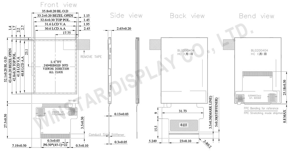
WFN0200A2T07ADNN000은 투과형과 반사형 디스플레이 모드를 결합한 첨단 반투과형 스크린(Transflective screen) 기술을 채택하여 다양한 조명 환경에서도 높은 시인성을 제공합니다. 이 2인치 세로형 모듈은 240x320 픽셀 해상도와 VA 광시야각을 갖추고 있어 야외 및 휴대용 장치에 적합합니다.

| 항목 | 치수 | 단위 |
|---|---|---|
| 크기 (대각선) | 2 | 인치 |
| 도트 매트릭스 (해상도) | 240 × RGB × 320(TFT) | dots |
| 모듈 치수 | 35.8 × 52.1 × 2.65 | mm |
| 활성 영역 | 30.60 × 40.80 | mm |
| 도트 피치 | 0.1275 × 0.1275 | mm |
| LCD 유형 | TFT, 검은색, 반투과성 | |
| 시야각 | 80/80/80/80 | |
| TFT 인터페이스 | 3/4serial 8/9/16/18bit MCU 3/4SPI+16/18BIT RGB |
|
| 역광 타입 | LED,백색 | |
| TFT 드라이버 IC | ST7789 또는 이와 동등한 | |
| 터치 패널 | 터치패널(스크린)이 없는 | |
| 표면 | 눈부심 | |
| 항목 | 기호 | 최소값 | 대표값 | 최대값 | 단위 |
|---|---|---|---|---|---|
| 작동 온도 | TOP | -20 | - | +70 | ℃ |
| 보관 온도 | TST | -30 | - | +80 | ℃ |
| 항목 | 기호 | 최소값 | 대표값 | 최대값 | 단위 |
|---|---|---|---|---|---|
| Digital Supply Voltage | VCI | 2.5 | 3.3 | 3.6 | V |
| Digital interface supple Voltage | IOVCC | 1.65 | 1.8 | 3.3 | V |
| Normal mode Current consumption | IDD | -- | 6 | 12 | mA |
| Level input voltage | VIH | 0.7IOVCC | IOVCC | V | |
| VIL | GND | 0.3IOVCC | V | ||
| Level output voltage | VOH | 0.8IOVCC | IOVCC | V | |
| VOL | GND | 0.2IOVCC | V |
| 항목 | 기호 | 최소값 | 대표값 | 최대값 | 단위 |
|---|---|---|---|---|---|
| LED 전류 | - | 60 | 80 | - | mA |
| LED 전압 | VLED+ | 2.8 | 3.2 | 3.3 | V |
| LED 수명 | - | 50,000 | - | - | Hr |
| Pin No | 기호 | 기능 | I/O |
|---|---|---|---|
| 1 | GND | Ground. | P |
| 2 | VCI | Supply voltage (3.3V). | P |
| 3 | IOVCC | Supply voltage (1.65-3.3V). | P |
| 4 | IM2 | MPU Parallel interface bus and serial interface select If use RGB Interface must select serial interface. Fix this pin at IOVCC and GND. |
I |
| 5 | IM1 | ||
| 6 | IM0 | ||
| 7 | RESET | This signal will reset the device and must be applied to properly initialize the chip. |
I |
| 8 | CS | Chip select input pin (“Low” enable). fix this pin at GND when not in use. |
I |
| 9 | DC(SPI-SCL) | -Display data/command selection pin in parallel interface. -This pin is used to be serial interface clock. DC=’1’: display data or parameter. DC=’0’: command data. -If not used, please fix this pin at GND. |
I |
| 10 | WR(SPI-RS) | -Write enable in MCU parallel interface. Display data/command selection pin in 4-line serial interface. Second Data lane in 2 data lane serial interface. -If not used, please fix this pin at GND. |
I |
| 11 | RD | Serves as a read signal and MCU read data at the rising edge. fix this pin at IOVCC or GND when not in use. |
I |
| 12 | VSYNC | Frame synchronizing signal for RGB interface operation. fix this pin at GND when not in use. |
I |
| 13 | HSYNC | Line synchronizing signal for RGB interface operation. fix this pin at GND when not in use. |
I |
| 14 | ENABLE | Data enable signal for RGB interface operation. fix this pin at GND when not in use. |
I |
| 15 | DOTCLK | Dot clock signal for RGB interface operation. Fix this pin at GND when not in use. |
I |
| 16 | SDA | Serial input signal. The data is latched on the rising edge of the SCL signal. fix this pin at GND when not in use. |
I |
| 17-34 | DB0-DB17 | 18-bit parallel bi-directional data bus for MCU system and RGB interface mode . Fix to GND level when not in use |
I/0 |
| 35 | SDO | SPI interface output pin. -The data is output on the falling edge of the SCL signal. -If not used, let this pin open. |
O |
| 36 | LEDA | Anode pin of backlight | P |
| 37 | LEDK1 | Cathode pin OF backlight | P |
| 38 | LEDK2 | Cathode pin OF backlight | P |
| 39 | LEDK3 | Cathode pin OF backlight | P |
| 40 | LEDK4 | Cathode pin OF backlight | P |
| 41 | XR(NC) | Touch panel Right Glass Terminal | A/D |
| 42 | YU(NC) | Touch panel Top Film Terminal | A/D |
| 43 | XL(NC) | Touch panel LEFT Glass Terminal | A/D |
| 44 | YD(NC) | Touch panel Bottom Film Terminal | A/D |
| 45 | GND | Ground. | P |

"모든 쿠키 허용"을 클릭하면 사이트 탐색을 개선하고, 사이트 사용을 분석하며, 마케팅 및 성능 노력에 도움을 주기 위해 쿠키를 귀하의 장치에 저장하는 데 동의한 것으로 간주됩니다. 이 주제에 대한 추가 정보는 당사의 정책에서 확인할 수 있습니다. 개인정보 보호정책