우리는 귀하의 프라이버시를 소중히 여깁니다
"모든 쿠키 허용"을 클릭하면 사이트 탐색을 개선하고, 사이트 사용을 분석하며, 마케팅 및 성능 노력에 도움을 주기 위해 쿠키를 귀하의 장치에 저장하는 데 동의한 것으로 간주됩니다. 이 주제에 대한 추가 정보는 당사의 정책에서 확인할 수 있습니다. 개인정보 보호정책


WO12864B는 2.8인치 COG 모노크롬 그래픽 LCD 디스플레이 모듈로, 128×64 dots 해상도를 제공합니다. ST7565P 컨트롤러 또는 호환 IC를 내장하고 있으며, 6800 8-bit, 8080 8-bit 병렬 인터페이스와 SPI 인터페이스를 지원하여 다양한 시스템에 적용할 수 있습니다.
동작 온도 범위는 -20℃~+70℃이며, 보관 온도 범위는 -30℃~+80℃입니다. COG(Chip On Glass) 구조를 적용하여 모듈 크기를 최소화하였으며, 설치 공간이 제한된 임베디드 장비 및 소형 디스플레이 애플리케이션에 적합합니다.
WO12864B 시리즈는 두 가지 두께 사양으로 제공됩니다.
► WO12864B : 두께 12.1 mm (Max)
► WO12864B1 : 두께 6.0 mm
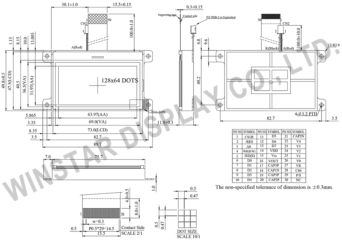
| 항목 | 치수 | 단위 |
|---|---|---|
| 표시 도트 수 | 128 x 64 | - |
| 모듈 치수 | 89.7 x 49.8 x 11.8 | mm |
| 보기 영역 | 69.0 x 36.5 | mm |
| 활성 영역 | 63.97 x 31.97 | mm |
| 도트 크기 | 0.47 x 0.47 | mm |
| 도트 피치 | 0.5 x 0.5 | mm |
| 듀티 | 1/65 , 1/9 Bias | |
| 역광 타입 | LED | |
| IC | ST7565P | |
| 인터페이스 | 6800/8080/4-Line SPI | |
| 항목 | 기호 | 최소값 | 대표값 | 최대값 | 단위 |
|---|---|---|---|---|---|
| 작동 온도 | TOP | -20 | - | +70 | ℃ |
| 보관 온도 | TST | -30 | - | +80 | ℃ |
| Power Supply Voltage | VDD | -0.3 | - | 3.6 | V |
| Power supply voltage (VDD standard) | V0,VOUT | -0.3 | - | 14.5 | V |
| Power supply voltage (VDD standard) | V1,V2,V3,V4 | -0.3 | - | V0+0.3 | V |
| 항목 | 기호 | 조건 | 최소값 | 대표값 | 최대값 | 단위 |
|---|---|---|---|---|---|---|
| Supply Voltage For Logic | VDD-VSS | - | 2.7 | - | 3.3 | V |
| Supply Voltage For LCM | V0-VSS | Ta=-20℃ Ta=25℃ Ta=70℃ |
9.5 9.2 8.95 |
9.8 9.45 9.2 |
10.5 9.8 9.45 |
V V V |
| Input High Volt. | VIH | - | 0.8 VDD | - | VDD | V |
| Input Low Volt. | VIL | - | VSS | - | 0.2VDD | V |
| Output High Volt. | VOH | IOUT=-0.5mA | 0.8VDD | - | VDD | V |
| Output Low Volt. | VOL | IOUT=0.5mA | VSS | - | 0.2VDD | V |
| Supply Current(No include LED Backlight) | IDD | - | - | 0.6 | 2.0 | mA |
| Pin No. | 기호 | Level | 설명 | |||||||||||||||
|---|---|---|---|---|---|---|---|---|---|---|---|---|---|---|---|---|---|---|
| 1 | /CS1B | I | This is the chip select signal. | |||||||||||||||
| 2 | /RES | I | When RES is set to “L”, the setting are initialized. | |||||||||||||||
| 3 | A0 | I | This is connect to the least significant bit of the normal MPU address bus, and it determines whether the data bits are data or command. A0 = “H”: Indicates that D0 to D7 are display data. A0 = “L”: Indicates that D0 to D7 are control data. |
|||||||||||||||
| 4 | /WR(R/W) | I | • When connected to 8080 series MPU, this pin is treated as the “/WR” signal of the 8080 MPU and is LOW-active. The signals on the data bus are latched at the rising edge of the /WR signal. • When connected to 6800 series MPU, this pin is treated as the “R/W” signal of the 6800 MPU and decides the access type : When R/W = “H”: Read. When R/W = “L”: Write. |
|||||||||||||||
| 5 | /RD(E) | I |
• When connected to 8080 series MPU, this pin is treated as the “/RD” signal of the 8080 MPU and is LOW-active. |
|||||||||||||||
| 6~13 | D0~D7 | I/O | Data bus line | |||||||||||||||
| 14 | VDD | Power supply | Power supply | |||||||||||||||
| 15 | VSS | Power supply | Ground | |||||||||||||||
| 16 | VOUT | O | DC/DC voltage converter. Connect a capacitor between this terminal and vss or VDD | |||||||||||||||
| 17 | CAP3P | O | DC/DC voltage converter. Connect a capacitor between this terminal and the CAP1N terminal. | |||||||||||||||
| 18 | CAP1N | O | DC/DC voltage converter. Connect a capacitor between this terminal and the CAP1P terminal. | |||||||||||||||
| 19 | CAP1P | O | DC/DC voltage converter. Connect a capacitor between this terminal and the CAP1N terminal. | |||||||||||||||
| 20 | CAP2P | O | DC/DC voltage converter. Connect a capacitor between this terminal and the CAP2N terminal. | |||||||||||||||
| 21 | CAP2N | O | DC/DC voltage converter. Connect a capacitor between this terminal and the CAP2P terminal. | |||||||||||||||
| 22~26 | V4~V0 | Power supply | This is a multi-level power supply for the liquid crystal drive. | |||||||||||||||
| 27 | VR | I | Output voltage regulator terminal. Provides the voltage between VSS and V0 through a resistive voltage divider. | |||||||||||||||
| 28 | C86 | I | This is the MPU interface selection pin. C86 = “H”: 6800 Series MPU interface. C86 = “L”: 8080 Series MPU interface |
|||||||||||||||
| 29 | P/S | I | This is the parallel data input/serial data input switch terminal. P/S = “H”: Parallel data input. P/S = “L”: Serial data input. The following applies depending on the P/S status:
/RD (E) and /WR (R/W) are fixed to either “H” or “L”. With serial data input, It is impossible read data from RAM |
|||||||||||||||
| 30 | NC | - | No connection. |

"모든 쿠키 허용"을 클릭하면 사이트 탐색을 개선하고, 사이트 사용을 분석하며, 마케팅 및 성능 노력에 도움을 주기 위해 쿠키를 귀하의 장치에 저장하는 데 동의한 것으로 간주됩니다. 이 주제에 대한 추가 정보는 당사의 정책에서 확인할 수 있습니다. 개인정보 보호정책