우리는 귀하의 프라이버시를 소중히 여깁니다
"모든 쿠키 허용"을 클릭하면 사이트 탐색을 개선하고, 사이트 사용을 분석하며, 마케팅 및 성능 노력에 도움을 주기 위해 쿠키를 귀하의 장치에 저장하는 데 동의한 것으로 간주됩니다. 이 주제에 대한 추가 정보는 당사의 정책에서 확인할 수 있습니다. 개인정보 보호정책


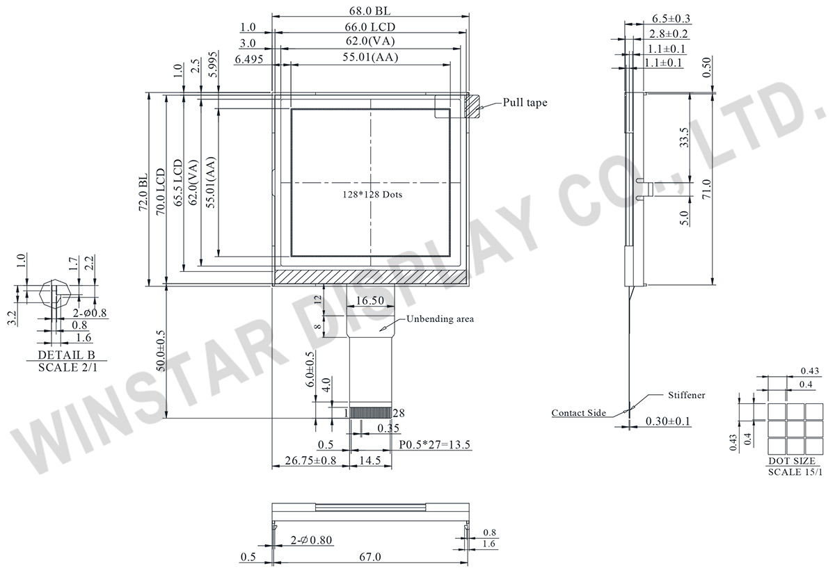
WO128128B는 3.06인치 128x128 모노크롬 그래픽 COG LCD 모듈로, ST75161 컨트롤러 IC를 탑재했습니다. 6800, 8080, 3선 SPI, 4선 SPI 및 I2C 인터페이스를 지원하며, 3.3V 로직 전원을 사용하고 1/128 Duty 및 1/12 Bias 구동 방식을 적용했습니다.
모듈 크기는 68.0 x 72.0 x 6.5 mm이며, 표시 영역(VA)은 62.0 x 62.0 mm, 유효 표시 영역(AA)은 55.01 x 55.01 mm입니다. LED 백라이트를 적용했으며, 동작 온도는 -20°C~+70°C, 보관 온도는 -30°C~+80°C입니다.
콤팩트한 COG 구조를 적용하여 모듈 두께를 줄였으며, 다양한 인터페이스를 지원해 임베디드 시스템에 손쉽게 통합할 수 있습니다. 128x128 모노크롬 그래픽 디스플레이는 공간 효율이 중요한 다양한 임베디드 장비에 적합합니다. 제품 공급 여부, 가격 또는 맞춤형 사양에 대한 문의는 상단의 제품 문의를 클릭한 후 문의 내용에 필요한 사항을 입력해 주시기 바랍니다.
Data source ref: WO128128B-TFH#
| 항목 | 치수 | 단위 |
|---|---|---|
| 표시 도트 수 | 128 x 128 | - |
| 모듈 치수 | 68.0 x 72.0 x 6.5 | mm |
| 보기 영역 | 62.0 x 62.0 | mm |
| 활성 영역 | 55.01 x 55.01 | mm |
| 도트 크기 | 0.4 x 0.4 | mm |
| 도트 피치 | 0.43 x 0.43 | mm |
| 듀티 | 1/128 DUTY,1/12 BIAS | |
| 역광 타입 | LED | |
| IC | ST75161 | |
| 인터페이스 | 6800/8080/3/4-Line SPI/I2C | |
| 항목 | 기호 | 최소값 | 대표값 | 최대값 | 단위 |
|---|---|---|---|---|---|
| 작동 온도 | TOP | -20 | - | +70 | ℃ |
| 보관 온도 | TST | -30 | - | +80 | ℃ |
| 전원 전압 | VDD | -0.3 | - | 4.0 | V |
| LCD 전원 전압 | V0-XV0 | -0.3 | - | 19 | V |
| 입력 전압 | VIN | -0.3 | - | VDD+0.3 | V |
| 항목 | 기호 | 조건 | 최소값 | 대표값 | 최대값 | 단위 |
|---|---|---|---|---|---|---|
| Supply Voltage For Logic | VDD-VSS | - | 3.0 | 3.3 | 3.6 | V |
| Supply Voltage For LCD | VOP | Ta=-20℃ Ta=25℃ Ta=70℃ |
- 14.8 - |
- 15.1 - |
- 15.4 - |
V V V |
| Input High Volt. | VIH | - | 0.7 VDD | - | VDD | V |
| Input Low Volt. | VIL | - | Vss | - | 0.3 VDD | V |
| Output High Volt. | VOH | - | 0.8 VDD | - | VDD | V |
| Output Low Volt. | VOL | - | Vss | - | 0.2 VDD | V |
| Supply Current | IDD | VDD=3.3V | - | - | 2.5 | mA |
| Pin No. | 기호 | 설명 |
|---|---|---|
| 1 | ESD GND | ESD Ground |
| 2 | VG | VG is the power of SEG-drivers. |
| 3 | V0 | Positive operating voltage of COM-drivers. |
| 4 | XV0 | Negative operating voltage of COM-drivers. |
| 5 | CA1P | DC/DC voltage converter |
| 6 | CA1N | |
| 7 | VDD | Power supply |
| 8 | VSS | Ground |
| 9 | COMSCN | Set scan direction of COM. |
| 10 | IF2 | These pins select interface operation mode. |
| 11 | IF1 | |
| 12 | IF0 | |
| 13 | CSB | Chip select input pin. |
| 14 | A0 | It determines whether the access is related to data or command. |
| 15 | ERD | Read / Write execution control pin. |
| 16 | RWR | Read / Write execution control pin. |
| 17-24 | RSTB | Hardware reset input pin |
| 25 | ERD | When using 8-bit parallel interface: 8080 or 6800 mode:8 bit bi-directional data bus When using serial interface : 4-line SPI or 3-line SPI mode D[7:4] : fix to “H” by VDD1. D[3:1] : serial input/output data (SDA). D[0] : serial input clock (SCL). D1 to D3 must be connected together (SDA) When using serial interface : I2C interface D[7] : SA[1], I2C slave address bit. Must be connected to VDD1 or VSS1. D[6] : SA[0], I2C slave address bit. Must be connected to VDD1 or VSS1. D[5:4] : fix to “H” by VDD1. D[3:2] : SDA_OUT, serial data and acknowledge output for the I2C interface. D[1] : SDA_IN, serial input data D[0] : SCL, serial input clock . D1 to D3 must be connected together (SDA) CSB must be fixed to “L” by VSS1. |
| 26 | A | Anode input for LED backlight. |
| 27 | K | Cathode input for LED backlight |
| 28 | ESD GND | ESD Ground |

"모든 쿠키 허용"을 클릭하면 사이트 탐색을 개선하고, 사이트 사용을 분석하며, 마케팅 및 성능 노력에 도움을 주기 위해 쿠키를 귀하의 장치에 저장하는 데 동의한 것으로 간주됩니다. 이 주제에 대한 추가 정보는 당사의 정책에서 확인할 수 있습니다. 개인정보 보호정책