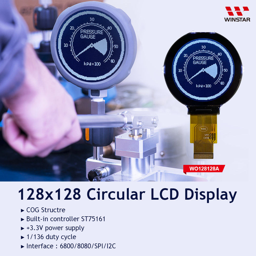
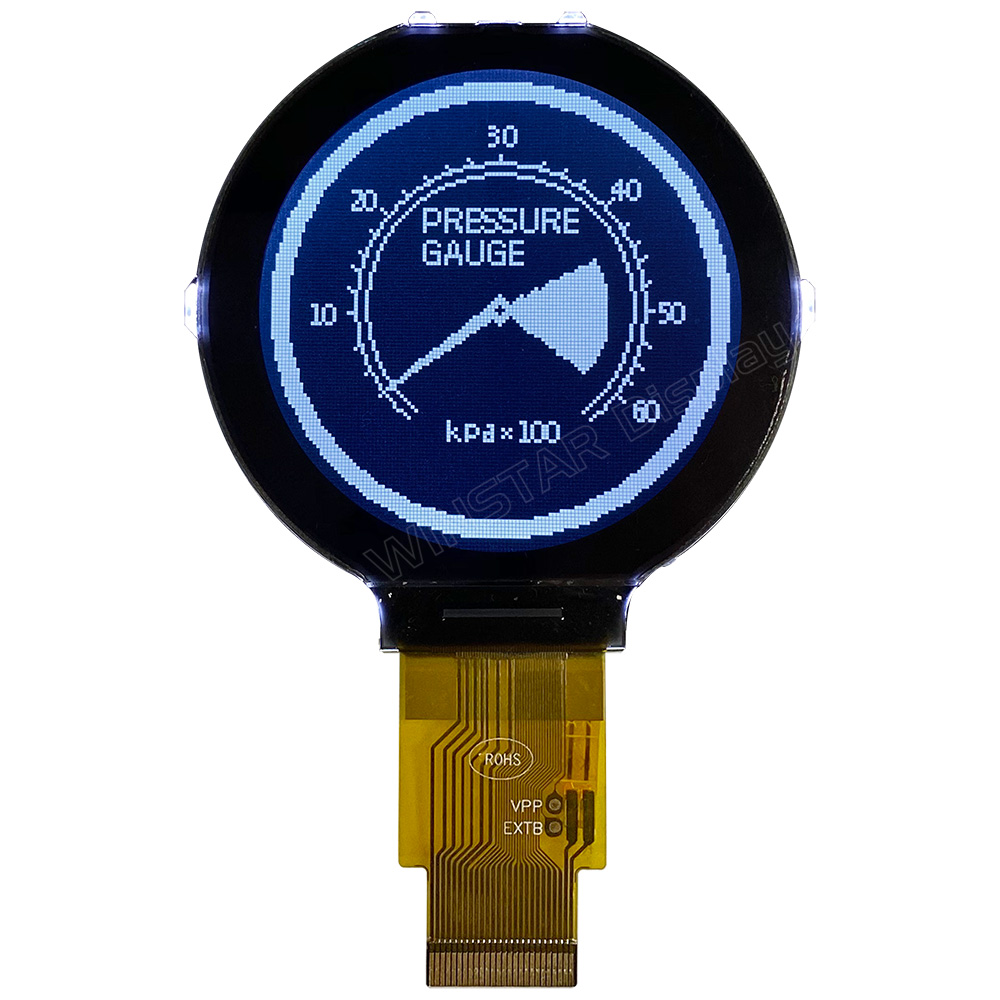
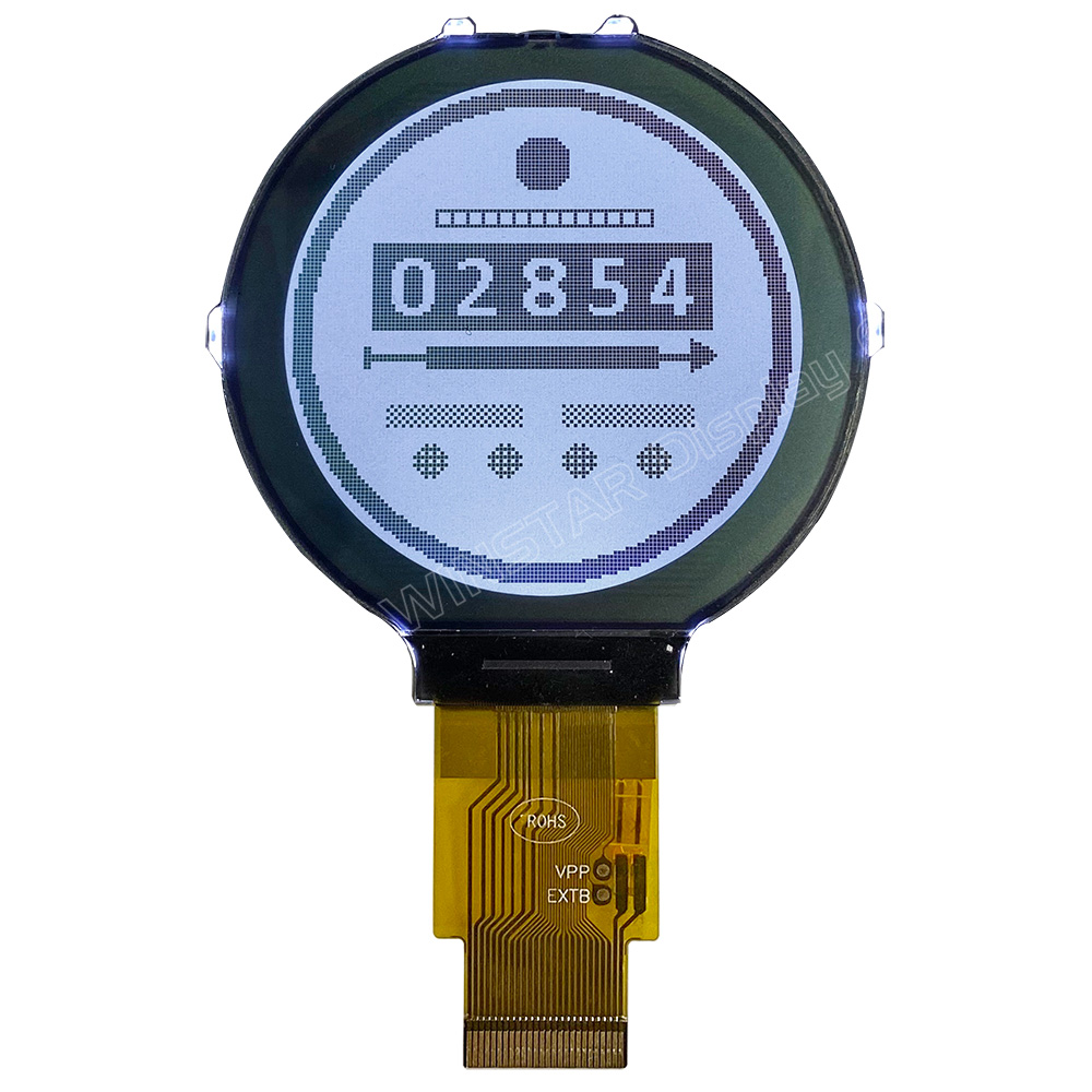
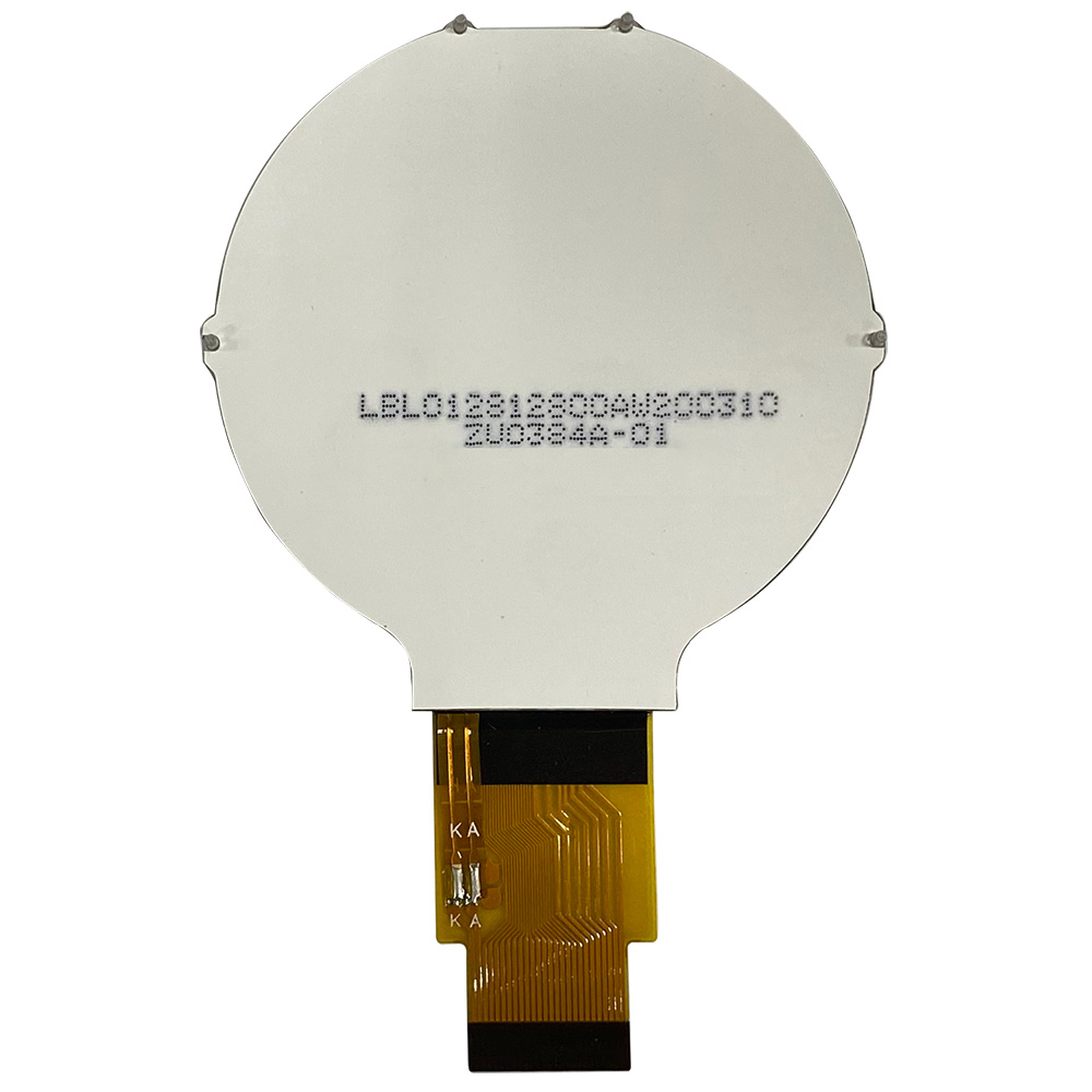
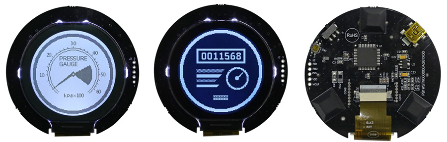
WO128128A ist ein grafisches COG-LCD-Modul mit 128x128 Punkten und ST75161 Controller-IC. Das Modul unterstützt 6800-/8080-Parallelschnittstellen, 3-Wire-/4-Wire-SPI sowie I2C. Die Blickrichtung ist auf 6 Uhr ausgelegt. Als Ansteuerung kommen 1/136 Duty und 1/12 Bias zum Einsatz.
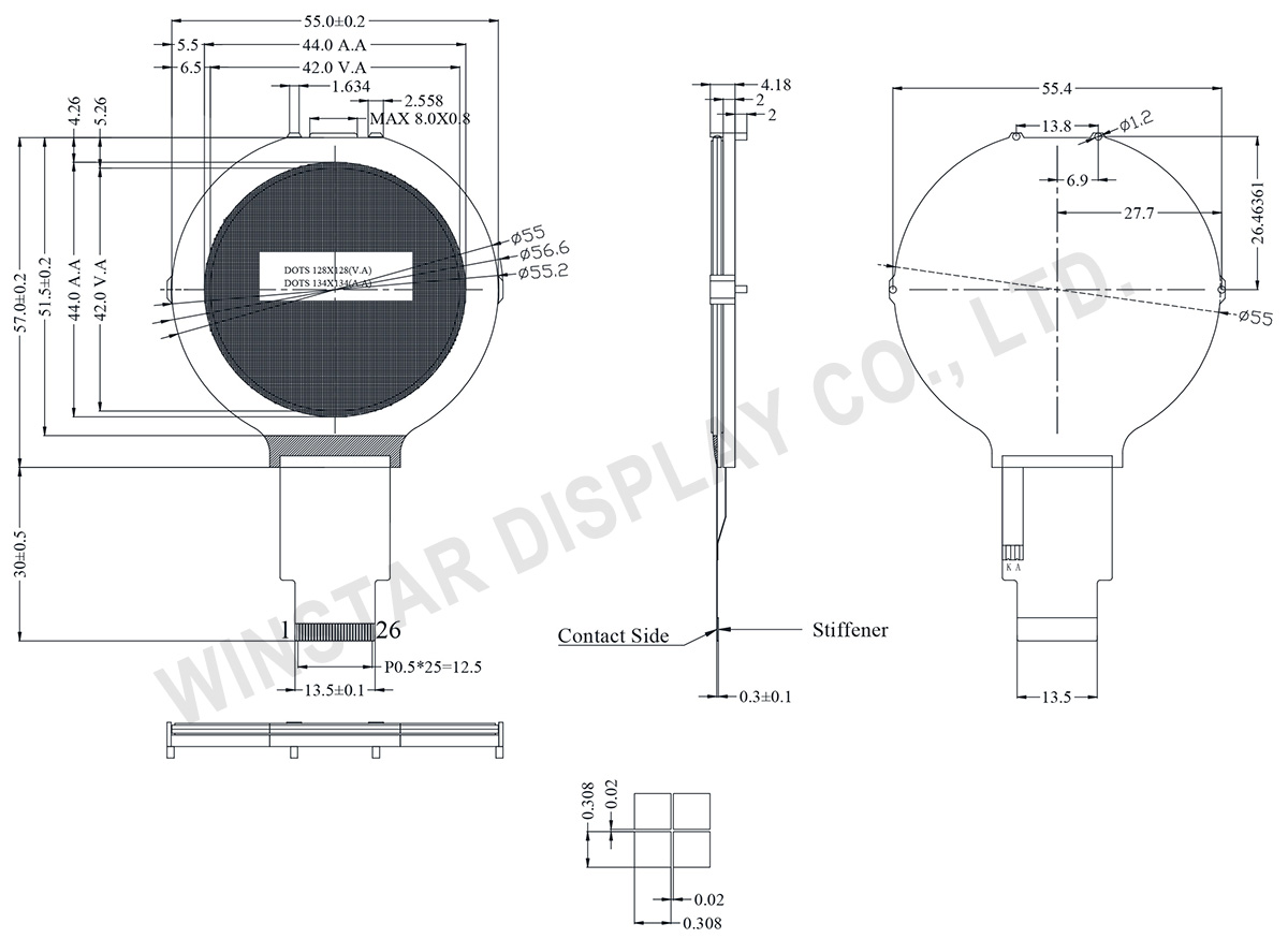
Die Modulabmessungen betragen 55,0 x 57,0 x 6,18 mm. Der Sichtbereich (VA) misst 42,0 x 42,0 mm, der aktive Bereich (AA) 44,0 x 44,0 mm. Die Logikversorgungsspannung (VDD) beträgt 2,7 V bis 3,3 V (typisch 3,0 V). Der Betriebstemperaturbereich reicht von -20 °C bis +70 °C, der Lagertemperaturbereich von -30 °C bis +80 °C.
Das WO128128A ist in zwei Displayvarianten erhältlich: WO128128A-TFH mit positivem FSTN-Display und weißer LED-Hintergrundbeleuchtung sowie WO128128A-TDI mit negativem FSTN-Display. Für beide Displayvarianten stehen USB Demo Kits zur Verfügung. Für Evaluierungsmuster, die Verfügbarkeit eines Demo Kits oder ein Angebot klicken Sie bitte auf „Produktanfrage“ und tragen Ihre Anforderungen im Feld „Nachricht“ ein.
Verfügbare Demo Kits
WWSTNUSBDEMO-00 – Für WO128128A-TFH
WWSTNUSBDEMO-01 – Für WO128128A-TDI
Zeichnung
Data source ref: WO128128A-TFH#
Technische Daten
Allgemeine Spezifikationen
Artikel
Ausmaß
Einheit
Anzahl der Bildpunkte
128 x 128
-
Abmaße der modul
55.0 x 57.0 x 6.18
mm
Anzeigebereich
42.0 x 42.0
mm
Aktiver Bereich
44.0 x 44.0
mm
Punktgröße
0.308 x 0.308
mm
Punktabstand
0.328 x 0.328
mm
Duty
1/136 DUTY,1/12 BIAS
Backlight-Typ
LED
IC
ST75161
Schnittstelle
68/80/4-Line SPI/I2C/9-bit 3-line serial interface
Absolute Grenzwerte
Artikel
Symbol
Mindestwert
typischer Wert
Maximalwert
Einheit
Betriebstemperatur
TOP
-20
-
+70
℃
Lagertemperatur
TST
-30
-
+80
℃
Power Supply Voltage
VDD
-0.3
-
4.0
V
LCD Power supply voltage
VLCD
-0.3
-
20
V
LCD Power supply voltage
V0-XV0
-0.3
-
19
V
Input voltage
VIN
-0.3
VDD+0.3
V
Elektrische Eigenschaften
Artikel
Symbol
Bedingung
Mindestwert
typischer Wert
Maximalwert
Einheit
Supply Voltage For Logic
VDD-VSS
-
2.7
3.0
3.3
V
Supply Voltage For LCD
VOP
Ta=-20℃
Ta=25℃
Ta=70℃
-
13.7
-
-
14.0
-
-
14.3
-
V
V
V
Input High Volt.
VIH
-
0.7 VDD
-
VDD
V
Input Low Volt.
VIL
-
Vss
-
0.3 VDD
V
Output High Volt.
VOH
-
0.8 VDD
-
VDD
V
Output Low Volt.
VOL
-
Vss
-
0.2 VDD
V
Supply Current
IDD
VDD=3.0V
-
-
2.0
mA
Schnittstelle Pin-Funktion
Pin No.
Symbol
Beschreibung
1
VG
VG is the power of SEG-drivers.
2
V0
Positive operating voltage of COM-drivers.
3
XV0
Negative operating voltage of COM-drivers.
4
CA1P
DC/DC voltage converter
5
CA1N
6
VDD
Power supply
7
VSS
Ground
8
COMSCN
Set scan direction of COM.
9
IF2
These pins select interface operation mode.
10
IF1
11
IF0
12
CSB
Chip select input pin.
13
A0
It determines whether the access is related to data or command.
14
ERD
Read / Write execution control pin.
15
RWR
Read / Write execution control pin.
16
RSTB
Hardware reset input pin
17-24
D0-D7
When using 8-bit parallel interface: 8080 or 6800 mode:8 bit bi-directional data bus When using serial interface : 4-line SPI or 3-line SPI mode
D[7:4] : fix to “H” by VDD1. D[3:1] : serial input/output data (SDA).
D[0] : serial input clock (SCL). D1 to D3 must be connected together (SDA)
When using serial interface : I2C interface
D[7] : SA[1], I2C slave address bit. Must be connected to VDD1 or VSS1. D[6] : SA[0], I2C slave address bit. Must be connected to VDD1 or VSS1.
D[5:4] : fix to “H” by VDD1. D[3:2] : SDA_OUT, serial data and acknowledge output for the I2C interface. D[1] : SDA_IN, serial input data D[0] : SCL, serial input clock .
D1 to D3 must be connected together (SDA)
CSB must be fixed to “L” by VSS1.
Durch Klicken auf „Alle Cookies zulassen“ stimmen Sie der Speicherung von Cookies auf Ihrem Gerät zu, um die Navigation auf der Website zu verbessern, die Nutzung der Website zu analysieren und unsere Marketing- und Leistungsbemühungen zu unterstützen. Weitere Informationen zu diesem Thema finden Sie in unserer Richtlinie. Datenschutzrichtlinie