

5.7" TFT LCD Module
Model No. WF57XTIACDNN0
►Size : 5.7 inch
►Resolution : 320 x 240 dots
►View Direction : 12H
►Interface: RGB
►Driver IC:HX8218+HX8615
►Control-Board : Option
►Brightness(cd/m²) : 900
►Frame Through Hole : No
►Touch Screen : No
►O-Film: Option
Description
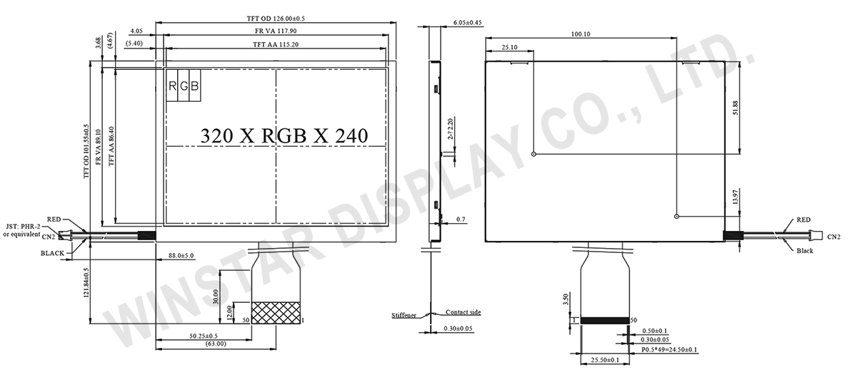
The WF57XTIACDNN0 is a 5.7-inch TFT LCD module with a resolution of 320 x 240 dots, boasting a brightness of 900 cd/m² and a contrast ratio of 300:1 (typical). It utilizes the HX8218+HX8615 driver IC, supporting 24-bit RGB interfaces. With a voltage power supply ranging from 3.2V to 3.4V (typical value: 3.3V), its module dimensions measure 126.00(W) × 101.55(H) mm, featuring an active area of 115.2 × 86.40 mm.
Featuring a 12 o'clock viewing direction, a 6 o'clock gray scale inversion direction, and a 4:3 aspect ratio, the WF57XTIACDNN0 is versatile for various applications. It operates efficiently within a temperature range of -20℃ to +70℃, with a storage temperature ranging from -30℃ to +80℃.
The brightness of this TFT display makes it ideal for Industrial Control and Monitoring applications, offering clear and easy-to-read displays for machine status, control panels, and monitoring systems, even in challenging environmental conditions. Moreover, its suitability for Outdoor Displays ensuring optimal visibility of information in bright light conditions without sacrificing clarity or legibility.
DRAWING
SPECIFICATIONS
Interface
| Pin No. | Symbol | I/O | Description |
|---|---|---|---|
| 1 | IF1 | I | Input data format control |
| 2 | IF2 | I | Input data format control |
| 3 | POL | O | Polarity Signal connect to VCOM driving circuit. |
| 4 | RESET | I | Hardware reset. |
| 5 | SPENA | I | Chip select |
| 6 | SPCL | I | Serial Clock |
| 7 | SPDA | I/O | Serial Data |
| 8 | B0 | I | Blue Data bit (LSB) |
| 9 | B1 | I | Blue Data bit |
| 10 | B2 | I | Blue Data bit |
| 11 | B3 | I | Blue Data bit |
| 12 | B4 | I | Blue Data bit |
| 13 | B5 | I | Blue Data bit |
| 14 | B6 | I | Blue Data bit |
| 15 | B7 | I | Blue Data bit(MSB) |
| 16 | G0 | I | Green Data bit(LSB) |
| 17 | G1 | I | Green Data bit |
| 18 | G2 | I | Green Data bit |
| 19 | G3 | I | Green Data bit |
| 20 | G4 | I | Green Data bit |
| 21 | G5 | I | Green Data bit |
| 22 | G6 | I | Green Data bit |
| 23 | G7 | I | Green Data bit(MSB) |
| 24 | R0 | I | Red Data bit(LSB) |
| 25 | R1 | I | Red Data bit |
| 26 | R2 | I | Red Data bit |
| 27 | R3 | I | Red Data bit |
| 28 | R4 | I | Red Data bit |
| 29 | R5 | I | Red Data bit |
| 30 | R6 | I | Red Data bit |
| 31 | R7 | I | Red Data bit(MSB) |
| 32 | Hsync | I | Horizontal synchronous signal |
| 33 | Vsync | I | Vertical synchronous signal |
| 34 | Data CLK | I | Dot data clock |
| 35 | AVDD | I | 4.5V~5.5V |
| 36 | AVDD | I | 4.5V~5.5V |
| 37 | Vcc | I | 3V~3.6V |
| 38 | Vcc | I | 3V~3.6V |
| 39 | NPC | O | NTSC/PAL mode Auto detection result H:NTSC/L:PAL |
| 40 | VGL | I | Gate off power |
| 41 | VGL | I | Gate off power |
| 42 | UD | I | Up/Down scan setting. H: Reverse scan / L: Normal scan |
| 43 | VGH | I | Gate on power |
| 44 | LRC | I | Shift direction of device internal shift register control. |
| 45 | GND | I | GROUND |
| 46 | VCOM | I | VCOM driving input |
| 47 | VCOM | I | VCOM driving input |
| 48 | ENB | I | Data enable input. Normally pull low. |
| 49 | GND | I | GROUND |
| 50 | GND | I | GROUND |
General Specifications
| Item | Dimension | Unit |
|---|---|---|
| Size | 5.7 | inch |
| Dot Matrix | 320 × RGB × 240 (TFT) | dots |
| Module dimension | 126.00(W) × 101.55(H) × 6.0(D) (MAX) | mm |
| Active area | 115.2 × 86.40 | mm |
| Dot pitch | 0.12 × 0.36 | mm |
| LCD type | TFT, Normally White, Transmissive | |
| View Direction | 12 o'clock | |
| Gray Scale Inversion Direction | 6 o'clock | |
| Aspect Ratio | 4:3 | |
| TFT Drive IC | HX8218+HX8615 or Equivalent | |
| Interface | 24-bit RGB | |
| Backlight Type | LED, Normally White | |
| Touch Panel | Without touch panel | |
| Surface | Glare | |
Absolute Maximum Ratings
| Item | Symbol | Min | Typ | Max | Unit |
|---|---|---|---|---|---|
| Operating Temperature | TOP | -20 | - | +70 | ℃ |
| Storage Temperature | TST | -30 | - | +80 | ℃ |
Electrical Characteristics
1. Operating conditions:| Item | Symbol | Condition | Min | Typ | Max | Unit |
|---|---|---|---|---|---|---|
| Supply Voltage For LCM | VCC | - | 3.2 | 3.3 | 3.4 | V |
| AVDD | 4.5 | 5.0 | 5.5 | |||
| Input High Volt. | VIH | - | 0.7 VCC | - | VCC | V |
| Input Low Volt. | VIL | - | 0 | - | 0.3 VCC | V |
| LCD Driving Supply Voltage | VGH | Ta=25℃ | 15 | 16 | 17 | V |
| VGL | -6 | -5 | -4 | |||
| VcomH | - | 4.5 | - | |||
| VcomL | - | -0.5 | - | |||
| Supply Current For LCM | IVCC | VCC=3.3V | - | 30 | 45 | mA |
2. LED driving conditions
| Parameter | Symbol | Min | Typ | Max | Unit |
|---|---|---|---|---|---|
| LED current | - | - | 140 | - | mA |
| Power Consumption | - | 1204 | - | 1470 | mW |
| LED voltage | VBL+ | 8.6 | 9.5 | 10.5 | V |
| LED Life Time | - | - | 50,000 | - | Hr |
