


Circular Display, 3.4" Circular Screen TFT LCD Display
Model No. WF0340ATYAB7MNN0
►Circular Display
►Size: 3.4 inch
►Resolution : 800 x 800 dots
►View Direction : Wide View (IPS)
►Interface : MIPI DSI
►Driver IC : ILI9881C
►Control-Board : No
►Brightness(cd/m2) : 300
►Frame Through Hole : No
►Touch Screen : No
Description
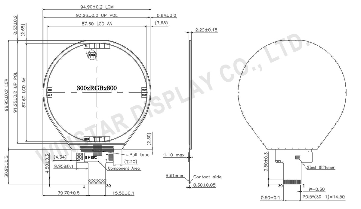
WF0340ATYAB7MNN0 is a 3.4-inch Circular Screen IPS TFT Display with a resolution of 800x800 dots. It uses IPS (In-plane Switching) technology to achieve fast and stable response time, higher frequency transmittance, and better color performance. The most significant advantage of IPS is the wider viewing angles of up: 85/ down: 85/ left: 85/ right: 85 degrees. This circular TFT display has the module dimensions of 94.9 x 96.95 mm and the active area of 87.6 x 87.6 mm. It boasts a built-in ILI9881C driver IC, supporting 4-wire MIPI interfaces. The contrast ratio of the module is 1200:1, the brightness is 300cd/m2 (typical value), the analog circuit voltage is 3.3V (typical value), and the logic circuit voltage is 1.8V.
The operating temperature range of this 3.4" LCD is from -20℃ to +70℃, and the storage temperature range covers from -30℃ to +80℃. The circular TFT LCD display is suitable for home appliances, electronic alarm clocks, cocktail machines, and other products requiring circular display screens.
The operating temperature range of this 3.4" LCD is from -20℃ to +70℃, and the storage temperature range covers from -30℃ to +80℃. The circular TFT LCD display is suitable for home appliances, electronic alarm clocks, cocktail machines, and other products requiring circular display screens.
DRAWING
SPECIFICATIONS
Interface
LCM PIN Definition
| Pin | Symbol | Function |
|---|---|---|
| 1 | VLED+ | VLED backlight anode. |
| 2 | VLED- | VLED backlight cathode. |
| 3 | VLED- | VLED backlight cathode. |
| 4 | VCI | Power supply for the analog power |
| 5 | IOVCC | Power supply for the logic power and I/O circuit (IOVCC = VDDI) |
| 6 | RESET | Reset signal(low active) (RESET=RESX) |
| 7 | TE | Tearing effect output |
| 8 | NC | No connection |
| 9 | GND | Power ground |
| 10 | D0P | MIPI-DSI data lane 0 positive input pin. |
| 11 | D0N | MIPI-DSI data lane 0 negative input pin |
| 12 | GND | Power ground |
| 13 | D1P | MIPI-DSI data lane 1 positive input pin. |
| 14 | D1N | MIPI-DSI data lane 1 negative input pin. |
| 15 | GND | Power ground |
| 16 | CLKP | MIPI-DSI data lane positive input pin. |
| 17 | CLKN | MIPI-DSI data lane negative input pin. |
| 18 | GND | Power ground |
| 19 | D2P | MIPI-DSI data lane 2 positive input pin. |
| 20 | D2N | MIPI-DSI data lane 2 negative input pin |
| 21 | GND | Power ground |
| 22 | D3P | MIPI-DSI data lane 3 positive input pin. |
| 23 | D3N | MIPI-DSI data lane 3 negative input pin |
| 24 | GND | Power ground |
| 25-30 | NC | No connection |
General Specifications
| Item | Dimension | Unit |
|---|---|---|
| Size | 3.4 | inch |
| Pixel Number | 800 × RGB × 800 (TFT) | dots |
| Module dimension | 94.9 (W) x 96.95 (H) x 2.22 (D) | mm |
| Active Area | 87.6 x 87.6 | mm |
| Pixel Pitch | 0.1095 x 0.1095 | mm |
| LCD type | TFT, Normally black, Transmissive | |
| Viewing Angle | 85/85/85/85 | |
| Driver IC | ILI9881C | |
| TFT Interface | 4-Lanes MIPI | |
| Backlight Type | LED, Normally White | |
| Touch Panel | Without Touch Panel | |
| Surface | Anti-Glare | |
Absolute Maximum Ratings
| Item | Symbol | Min | Typ | Max | Unit |
|---|---|---|---|---|---|
| Operating Temperature | TOP | -20 | - | +70 | ℃ |
| Storage Temperature | TST | -30 | - | +80 | ℃ |
| Power Supply voltage 1 | VCI~GND | >-0.3 | - | +3.6 | V |
| Power Supply voltage 2 | IOVCC~GND | -0.3 | - | +3.3 | V |
| Logic Input Voltage Range | VIN | -0.3 | - | IOVCC+0.3 | V |
| Logic Output Voltage Range | VO | -0.3 | - | IOVCC+0.3 | V |
Electrical Characteristics
| Item | Symbol | Min | Typ | Max | Unit |
|---|---|---|---|---|---|
| Supply voltage for analog circuit | VCI | 2.5 | 3.3 | 3.6 | V |
| Supply voltage for logic circuit | IOVCC | 1.65 | 1.8 | 3.3 | V |
| Current for VCI | I-vci | - | 20 | 30 | mA |
| Current for IOVCC | I-iovcc | - | 20 | 30 | mA |
| Input voltage “H” level | VIH | 0.7*IOVCC | - | IOVCC | V |
| Input voltage “L” level | VIL | GND | - | 0.3*IOVCC | V |
| Output voltage “H” level | VOH | 0.8*IOVCCI | - | IOVCC | V |
| Output voltage “L” level | VOL | GND | - | 0.2*IOVCC | V |
