

2.4" SPI TFT LCD Display Module 240x320 ST7789V with RTP
Model No. WF24MTLAJDNT0
►Size: 2.4 inch
►Resolution : 240×320 dots
►View Direction:6H
►SPI Interface (SPI TFT Display, SPI LCD, SPI Display)
►Driver IC:ST7789V
►Control-Board: No
►Brightness(cd/m²): 350
►Frame Through Hole: No
►Touch Screen: Resistive Touch Screen
Description
WF24MTLAJDNT0 is a 2.4-inch portrait mode SPI TFT-LCD display module with Resistive Touch Screen (RTP); resolution 240x320 pixels. This module is built-in with ST7789V IC; it supports 4-Line SPI interface, supply voltage for analog (Vcc) range from 2.4V to 3.6V, typical value 3.3V. The SPI interface allows for easy communication between the TFT LCD display and the host device, providing a reliable and efficient connection. This module is having anti-glare surface panel, view direction 6 o'clock, gray scale inversion 12 o'clock, contrast ratio 500:1.
WF24MTLAJDNT0 module is a Portrait mode TFT-LCD featured with brightness 350 nits (typical value). And with low power consumption, this display helps to extend battery life, making it an excellent choice for portable devices. The module also is available for without touch screen option part no. WF24MTLAJDNN0. The working temperatures for WF24M model is from -20°C to +70°C; its storage temperatures range from -30°C to +80°C.
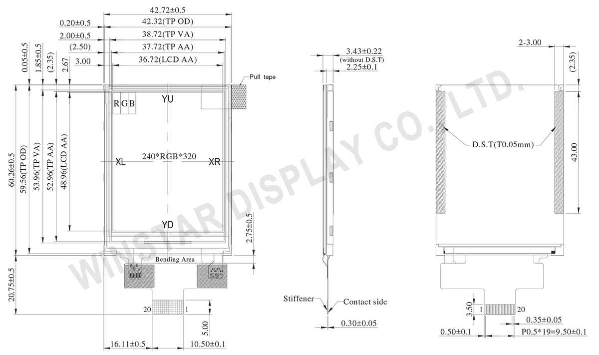
DRAWING
SPECIFICATIONS
Interface
LCM PIN Definition
| NO | Symbol | Function | ||||||||||||||||||
|---|---|---|---|---|---|---|---|---|---|---|---|---|---|---|---|---|---|---|---|---|
| 1 | GND | Ground | ||||||||||||||||||
| 2 | VLED+ | Anode of LED backlight. | ||||||||||||||||||
| 3 | VLED- | Cathode of LED backlight. | ||||||||||||||||||
| 4 | GND | Ground | ||||||||||||||||||
| 5 | VCC | Power supply | ||||||||||||||||||
| 6 | RESET | System reset pin. (RESX) signal is active low |
||||||||||||||||||
| 7 | SDA | When IM3: Low, SPI interface input/output pin. When IM3: High, SPI interface input pin. The data is latched on the rising edge of the SCL signal. If not used, please fix this pin at VDDI or DGND level. |
||||||||||||||||||
| 8 | DCX(SCL) | This pin is used to be serial interface clock. DCX=’1’: display data or parameter. DCX=’0’: command data. If not used, please fix this pin at VDDI or DGND. |
||||||||||||||||||
| 9 | CSX | Chip selection pin Low enable. High disable. |
||||||||||||||||||
| 10 | WRX(D/CX) | Display data/command selection pin in 4-line serial interface. Second Data lane in 2 data lane serial interface. If not used, please fix this pin at VDDI or DGND. |
||||||||||||||||||
| 11 | GND | Ground | ||||||||||||||||||
| 12 | SDO(DOUT) | SPI interface output pin. The data is output on the falling edge of the SCL signal. If not used, let this pin open. |
||||||||||||||||||
| 13 | TE | Tearing effect signal is used to synchronize MCU to frame memory writing. If not used, please let this pin open |
||||||||||||||||||
| 14 | IM3 | The MCU interface mode select.
|
||||||||||||||||||
| 15 | GND | Ground | ||||||||||||||||||
| 16 | XR | Right electrode | ||||||||||||||||||
| 17 | YD | Bottom electrode | ||||||||||||||||||
| 18 | XL | Left electrode | ||||||||||||||||||
| 19 | YU | Top electrode | ||||||||||||||||||
| 20 | GND | Ground |
General Specifications
| Item | Dimension | Unit |
|---|---|---|
| Size | 2.4 | inch |
| Dot Matrix | 240 × RGB × 320(TFT) | dots |
| Module dimension | 42.72(W) × 60.26(H) × 3.43(D) | mm |
| Active area | 36.72 × 48.96 | mm |
| Dot pitch | 0.153 × 0.153 | mm |
| LCD type | TFT, Normally White, Transmissive | |
| Interface | SPI | |
| TFT Driver IC | ST7789V or Equivalent | |
| View Direction | 6 o'clock | |
| Gray Scale Inversion Direction | 12 o'clock | |
| Aspect Ratio | Portrait | |
| Backlight Type | LED, Normally White | |
| Touch Panel | Resistive Touch Screen | |
| Surface | Anti-Glare | |
Absolute Maximum Ratings
| Item | Symbol | Min | Typ | Max | Unit |
|---|---|---|---|---|---|
| Operating Temperature | TOP | -20 | - | +70 | ℃ |
| Storage Temperature | TST | -30 | - | +80 | ℃ |
Electrical Characteristics
| Item | Symbol | Condition | Min | Typ | Max | Unit |
|---|---|---|---|---|---|---|
| Supply Voltage For Analog | Vcc | - | 2.4 | 3.3 | 3.6 | V |
| Supply Current For LCM | Icc | - | - | 6.4 | 9.6 | mA |
Search keyword: tft 2.4, tft 2.4", 2.4 tft lcd, 2.4" tft lcd, 2.4 inch tft lcd, tft lcd 2.4, 2.4 tft display, 2.4" tft display, 2.4 inch tft display, tft display 2.4, tft display 2.4", 240x320 lcd
