")


 - WF43QTIBEDBND")


 - WG12232J")
 - WG12232K")
我们重视您的隐私
通过点击「允许所有 Cookie」,代表您同意在您的设备上存储 Cookie 以增强网站浏览体验、分析网站使用情况并协助我们的营销和网站效能优化工作。您可以在我们的隐私权政策中找到有关于此的更多信息。
 - WF18FTZAADNN0")
 - WF18FTZAADNN0")
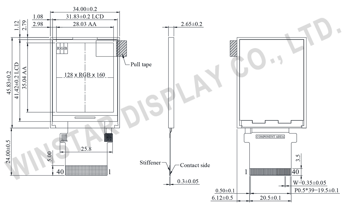
WF18FTZAADNN0是一款分辨率为128x160像素,1.77寸的TFT液晶显示模块。此模块内建ST7735S IC,支持MCU或SPI接口。WF18FTZAADNN0的模块尺寸为34.0 x 45.83 mm,有效区域(AA)为28.03 x 35.04 mm,电源电压为2.5V至4.8V(典型值为2.75V)。模块亮度为400 nits(典型值);对比度 500:1。
WF18FTZAADNN0是直屏模式的O-Film广视角TFT模块,其视角方向为6点钟,灰阶反转方向为12点钟方向。该模块的工作温度是-20℃至+70℃,储存温度为-30℃至+80℃。
| 项目 | 规格 | 单位 |
|---|---|---|
| 显示尺寸(对角线) | 1.77 | 寸 |
| 分辨率 | 128 × RGB × 160(TFT) | dots |
| 模块尺寸 | 34.0(W) × 45.83(H) × 2.65(D) | mm |
| 有效区域(AA) | 28.03 × 35.04 | mm |
| 点间距 | 0.073 × 0.219 | mm |
| LCD 类型 | TFT, 平常白, 透射式 | |
| 视角 | 6点钟方向 | |
| 灰阶反转 | 12点钟方向 | |
| 长宽比 | 直屏 | |
| IC | ST7735S | |
| 背光类型 | LED, 平常白 | |
| 触控面板类型 | 无触控面板 | |
| 表面 | 防眩光 | |
| 项目 | 符号 | 最小值 | 典型值 | 最大值 | 单位 |
|---|---|---|---|---|---|
| 工作温度 | TOP | -20 | - | 70 | ℃ |
| 储存温度 | TST | -30 | - | 80 | ℃ |
| 项目 | 符号 | 条件 | 最小值 | 典型值 | 最大值 | 单位 |
|---|---|---|---|---|---|---|
| 模拟供电电压 | VCI | - | 2.5 | 2.75 | 4.8 | V |
| 接口工作电压 | IOVCC | - | 1.65 | 1.8 | 3.7 | V |
| LCM供电电流 | ICI(mA) | - | - | 0.9 | 2 | mA |
| 参数 | 符号 | 最小值 | 典型值 | 最大值 | 单位 |
|---|---|---|---|---|---|
| LED电流 | - | 40 | - | mA | |
| 耗电量 | - | 124 | - | mW | |
| LED电压 | VBL+ | 2.9 | 3.1 | 3.4 | V |
| LED 寿命 | - | 50,000 | - | Hr |
| Pin | 符号 | I/O | 功能说明 | |||||||||||||||
|---|---|---|---|---|---|---|---|---|---|---|---|---|---|---|---|---|---|---|
| 1 | VLED- | P | Back light cathode | |||||||||||||||
| 2 | VLED | P | Back light anode | |||||||||||||||
| 3 | IM0 | I | - MCU Parallel Interface Type Selection -If Not Used, Please Fix this Pin at VDDI or DGND Level.
|
|||||||||||||||
| 4 | IM1 | |||||||||||||||||
| 5 | IM2 | I | MCU Parallel Interface Bus and Serial Interface select IM2='1', Parallel Interface IM2='0', Serial Interface |
|||||||||||||||
| 6 | RESET | P | Reset signal | |||||||||||||||
| 7-12 | NC | - | No Connect | |||||||||||||||
| 13-28 | DB15-DB0(SPI_SDA) | I/O | DB15:0] are used as MCU parallel interface data bus. -DBis the serial input/output signal in serial interface mode. -In serial interface, DB15:1] are not used and should be fixed at VDDI or DGND level. |
|||||||||||||||
| 29 | NC | - | No Connect | |||||||||||||||
| 30 | RD | I | Read Enable in 8080 MCU Parallel Interface. -If not used, please fix this pin at VDDI or DGND level. |
|||||||||||||||
| 31 | WR | I | Serial clock -Write Enable in MCU Parallel Interface. -If not used, please fix this pin at VDDI or DGND level. |
|||||||||||||||
| 32 | D/C(SPI_SCL) | I | -Display data/command Selection Pin in MCU Interface. -D/CX='1': Display Data or Parameter. -D/CX='0': Command Data. -In Serial Interface, this is used as SCL. -If not used, please fix this pin at VDDI or DGND level. |
|||||||||||||||
| 33 | CS(SPI_CS) | I | Chip enable | |||||||||||||||
| 34 | IOVCC | P | Interface Operation Voltage | |||||||||||||||
| 35 | VCI | P | Analog Supply Voltage | |||||||||||||||
| 36 | GND | P | Ground | |||||||||||||||
| 37-40 | NC | - | No Connect |

通过点击「允许所有 Cookie」,代表您同意在您的设备上存储 Cookie 以增强网站浏览体验、分析网站使用情况并协助我们的营销和网站效能优化工作。您可以在我们的隐私权政策中找到有关于此的更多信息。