
 + 프레임으로 - WEF012864U")

")
우리는 귀하의 프라이버시를 소중히 여깁니다
"모든 쿠키 허용"을 클릭하면 사이트 탐색을 개선하고, 사이트 사용을 분석하며, 마케팅 및 성능 노력에 도움을 주기 위해 쿠키를 귀하의 장치에 저장하는 데 동의한 것으로 간주됩니다. 이 주제에 대한 추가 정보는 당사의 정책에서 확인할 수 있습니다. 개인정보 보호정책

- WEO012864U")
- WEO012864U")
- WEO012864U")
- WEO012864U")
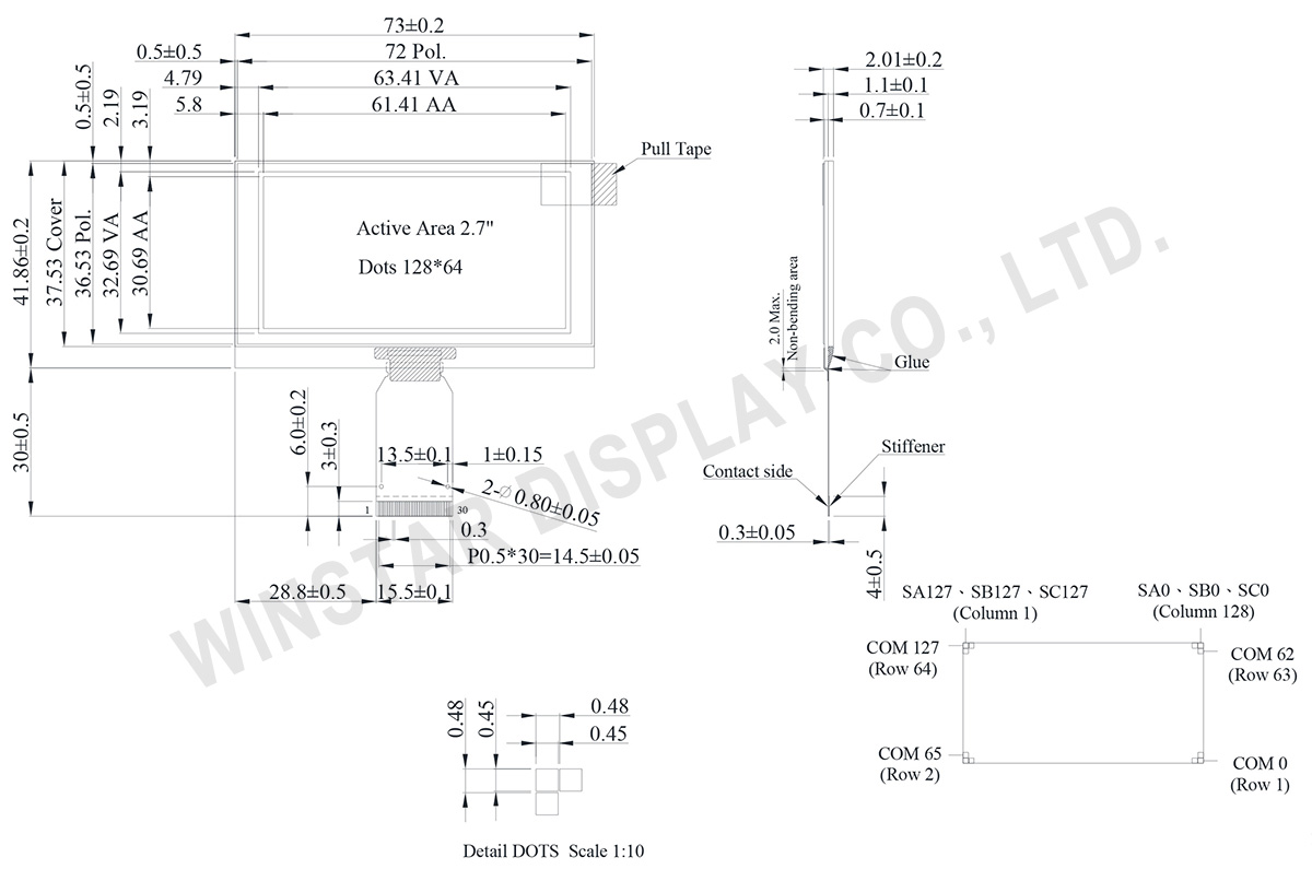
WEO012864U는 2.7인치의 인기있는 그래픽 OLED 디스플레이로, COG 구조와 128x64 도트의 해상도를 갖추고 있습니다. 이 모듈은 SSD1357 IC로 제작되었으며, 6800/8080 8비트 병렬, I2C 및 4-Wire SPI 인터페이스를 지원하며, 논리용 전압은 3V이며 1/64 듀티 사이클을 갖추고 있습니다.
WEO012864U OLED 모듈은 10,000:1의 높은 대비 비율과 4비트 그레이스케일 이미지를 지원합니다. 이는 벽/미터 장치, 가정용 애플리케이션, 금융 POS, 클라우드/IoT 시스템, 지능형 기기, 에너지 시스템, 통신 시스템, 의료 기기 등에 이상적입니다. WEO012864U 모듈은 -40℃에서 80℃까지의 온도에서 작동할 수 있으며, 저장 온도는 -40℃에서 85℃까지 범위합니다.
유사한 OLED 패널은 WEF012864U 시리즈에서도 제공되며, 여기에는 메탈 프레임이 포함되지만 PCB는 제외되어 있습니다. 그리고 WEP012864U 시리즈는 메탈 프레임과 PCB가 모두 포함되어 있습니다. 터치 기능이 필요한 경우 WEP012864U-CTP 시리즈를 선택하는 것을 고려해 주세요.
| 항목 | 치수 | 단위 |
|---|---|---|
| 도트 매트릭스 | 128 x 64 | Dots |
| 모듈 치수 | 73.0 × 41.86 × 2.01 | mm |
| 활성 영역 | 61.41 × 30.69 | mm |
| 도트 크기 | 0.45 × 0.45 | mm |
| 도트 피치 | 0.48 × 0.48 | mm |
| 디스플레이 모드 | 패시브 매트릭스 | |
| 디스플레이 색상 | Monochrome | |
| Drive Duty | 1/64 Duty | |
| IC | SSD1357 | |
| 인터페이스 | 6800, 8080, SPI, I2C | |
| 크기 | 2.7 인치 | |
| Parameter | 기호 | 최소값 | 최대값 | 단위 |
|---|---|---|---|---|
| Supply Voltage for Logic | VDD | -0.3 | 4.0 | V |
| Supply Voltage for Display | VCC | 0 | 15.0 | V |
| 작동 온도 | TOP | -40 | 80 | °C |
| 보관 온도 | TSTG | -40 | 85 | °C |
| 항목 | 기호 | 조건 | 최소값 | 대표값 | 최대값 | 단위 |
|---|---|---|---|---|---|---|
| Supply Voltage for Logic | VDD | - | 2.8 | 3.0 | 3.3 | V |
| Supply Voltage for Display | VCC | - | 9.5 | 10.0 | 10.5 | V |
| High Level Input | VIH | - | 0.8×VDD | - | - | V |
| Low Level Input | VIL | - | - | - | 0.2×VDD | V |
| High Level Output | VOH | - | 0.9×VDD | - | - | V |
| Low Level Output | VOL | - | - | - | 0.1×VDD | V |
| 50% Check Board operating Current | VCC =10.0V | - | 46 | 69 | mA | |
| No. | 기호 | 기능 | |||||||||||||||
|---|---|---|---|---|---|---|---|---|---|---|---|---|---|---|---|---|---|
| 1 | NC(GND) | No connection. | |||||||||||||||
| 2 | VSS | Ground of Logic Circuit. This is a ground pin. It also acts as a reference for the logic pins. It must be connected to external ground. |
|||||||||||||||
| 3 | VCC | Power supply for panel driving voltage. This is also the most positive power voltage supply pin. | |||||||||||||||
| 4 | VCOMH | Voltage Output High Level for COM Signal. This pin is the input pin for the voltage output high level for COM signals. A tantalum capacitor should be connected between this pin and VSS. |
|||||||||||||||
| 5 | VLSS | Ground of Analog Circuit These are the analog ground pins. They should be connected to VSS externally. |
|||||||||||||||
| 6~13 | D7~D0 | These pins are bi-directional data bus connecting to the MCU data bus. Unused pins are recommended to tie LOW. When serial interface mode is selected, D0 will be the serial clock input: SCLK; D1 will be the serial data input: SDIN and D2 should be kept NC. When I2C mode is selected, D2, D1 should be tied together and serve as SDAout, SDAin in application and D0 is the serial clock input, SCL. |
|||||||||||||||
| 14 | E/RD# | This pin is MCU interface input. When 6800 interface mode is selected, this pin will be used as the Enable (E) signal. Read/write operation is initiated when this pin is pulled HIGH and the chip is selected. When 8080 interface mode is selected, this pin receives the Read (RD#) signal. Read operation is initiated when this pin is pulled LOW and the chip is selected. When serial or I2C interface is selected, this pin must be connected to VSS. |
|||||||||||||||
| 15 | R/W# | This pin is read / write control input pin connecting to the MCU interface. When 6800 interface mode is selected, this pin will be used as Read/Write (R/W#) selection input. Read mode will be carried out when this pin is pulled HIGH and write mode when LOW. When 8080 interface mode is selected, this pin will be the Write (WR#) input. Data write operation is initiated when this pin is pulled LOW and the chip is selected. When serial or I2C interface is selected, this pin must be connected to VSS. |
|||||||||||||||
| 16 17 |
BS1 BS2 |
Communicating Protocol Select. These pins are MCU interface selection input. See the following table:
|
|||||||||||||||
| 18 | D/C# | This pin is Data/Command control pin connecting to the MCU. When the pin is pulled HIGH, the data at D[7:0] will be interpreted as data. When the pin is pulled LOW, the data at D[7:0] will be transferred to a command register. In I2C mode, this pin acts as SA0 for slave address selection. When 3-wire serial interface is selected, this pin must be connected to VSS. |
|||||||||||||||
| 19 | CS# | Chip Select This pin is the chip select input. The chip is enabled for MCU communication only when CS# is pulled low. |
|||||||||||||||
| 20 | RES# | This pin is reset signal input. When the pin is pulled LOW, initialization of the chip is executed. Keep this pin pull HIGH during normal operation. |
|||||||||||||||
| 21 | FR | Frame Frequency Triggering Signal This pin will send out a signal that could be used to identify the driver status. Nothing should be connected to this pin. It should be left open individually. |
|||||||||||||||
| 22 | IREF | This pin is the segment output current reference pin. IREF is supplied externally. |
|||||||||||||||
| 23 | N.C. | Reserved Pin The N.C. pin between function pins is reserved for compatible and flexible design. |
|||||||||||||||
| 24 | VDD | Power Supply for I/O Pin. This pin is a power supply pin of I/O buffer. It should be connected to VCI or external source. All I/O signal should have VIH reference to VDDIO. When I/O signal pins (BS0~BS1, D0~D7, control signals…) pull high, they should be connected to VDDIO. |
|||||||||||||||
| 25 | VP | Power Supply for Core Logic Circuit This is a voltage supply pin. It can be supplied externally (within the range of 2.4~2.6V) or regulated internally from VCI. A capacitor should be connected between this pin & VSS under all circumstances. |
|||||||||||||||
| 26 | VDD | Power Supply for Operation. This is a voltage supply pin. It must be connected to external source & always be equal to or higher than VDD & VDDIO. |
|||||||||||||||
| 27 | VSL | Voltage Output Low Level for SEG Signal This is segment voltage (output low level) reference pin. This pin has to connect with resistor and diode to ground (details depends on application). |
|||||||||||||||
| 28 | VLSS | Ground of Analog Circuit These are the analog ground pins. They should be connected to VSS externally. |
|||||||||||||||
| 29 | VCC | Power Supply for OEL Panel These are the most positive voltage supply pin of the chip. They must be connected to external source. |
|||||||||||||||
| 30 | NC(GND) | No connection |

"모든 쿠키 허용"을 클릭하면 사이트 탐색을 개선하고, 사이트 사용을 분석하며, 마케팅 및 성능 노력에 도움을 주기 위해 쿠키를 귀하의 장치에 저장하는 데 동의한 것으로 간주됩니다. 이 주제에 대한 추가 정보는 당사의 정책에서 확인할 수 있습니다. 개인정보 보호정책