
私たちはあなたのプライバシーを大切にします
「すべてのクッキーを許可」をクリックすると、サイトのナビゲーションを向上させ、サイト使用状況を分析し、マーケティングおよびパフォーマンスの取り組みを支援するために、クッキーをデバイスに保存することに同意したことになります。この件に関する詳細情報は、ポリシーをご覧ください。プライバシーポリシー


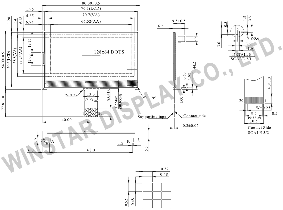
WO12864Hは、2.93インチ 128x64 STN COG LCDモジュールです。ST7567 コントローラ IC を搭載し、6800、8080、または 4線式 SPI インターフェース仕様をご用意しています。
モジュール外形寸法は 80.0 x 54.0 x 9.5 mm、VAサイズは 70.7 x 38.8 mm、有効表示エリアは 66.52 x 33.24 mmです。表示は1/65 Duty、1/9 Biasで駆動し、3.0 V~3.6 Vのロジック電源に対応しています。
動作温度範囲は -20°C~+70°C、保存温度範囲は -30°C~+80°Cで、産業機器、計測機器、医療機器、携帯型機器、各種組み込み機器向け表示用途に適しています。
| 項目 | 標準値 | 単位 |
|---|---|---|
| 表示ドット数 | 128 x 64 | - |
| モジュールサイズ | 80.0 x 54.0 x 9.5 | mm |
| 表示エリア | 70.7 x 38.8 | mm |
| 有効エリア | 66.52 x 33.24 | mm |
| ドットサイズ | 0.48 x 0.48 | mm |
| ドットピッチ | 0.52 x 0.52 | mm |
| 駆動方法 | 1/65 , 1/9 Bias | |
| バックライトタイプ | LED | |
| IC | ST7567 | |
| インターフェイス | 6800/8080/4-Line SPI | |
| 項目 | 記号 | 最小値 | 典型値 | 最大値 | 単位 |
|---|---|---|---|---|---|
| 操作温度 | TOP | -20 | - | +70 | ℃ |
| 保存温度 | TST | -30 | - | +80 | ℃ |
| 入力電圧 | VI | -0.3 | - | VDD+0.3 | V |
| デジタル電源電圧 | VDD,VSS | -0.3 | - | 3.6 | V |
| LCD電源電圧 | V0-XV0 | -0.3 | - | 16 | V |
| 項目 | 記号 | 条件 | 最小値 | 典型値 | 最大値 | 単位 |
|---|---|---|---|---|---|---|
| ロジック電源電圧 | VDD-VSS | - | 3.0 | 3.3 | 3.6 | V |
| LCM供給電圧 | XV0-V0 | Ta=-20℃ Ta=25℃ Ta=70℃ |
- - - |
- 10.0 - |
- - - |
V V V |
| 高レベル入力電圧 | VIH | - | 0.7 VDD | - | VDD | V |
| 低レベル入力電圧 | VIL | - | VSS | - | 0.3VDD | V |
| 高レベル出力電圧 | VOH | - | 0.8VDD | - | VDD | V |
| 低レベル出力電圧 | VOL | - | VSS | - | 0.2VDD | V |
| 供給電流 | IDD | VDD=3.3V | - | 2.0 | - | mA |
| Pin No. | 記号 | Level | 説明 | ||||||||||||
|---|---|---|---|---|---|---|---|---|---|---|---|---|---|---|---|
| 1 | PSB | I | PSB selects the interface type: Serial or Parallel. | ||||||||||||
| 2 | C86 | I | C86 selects the microprocessor type in parallel interface mode.
|
||||||||||||
| 3 | VG | Power | VG is the LCD driving voltage for segment circuits. | ||||||||||||
| 4 | XV0 | Power | XV0 is the LCD driving voltage for common circuits at positive frame. | ||||||||||||
| 5 | V0 | Power | V0 is the LCD driving voltage for common circuits at negative frame. | ||||||||||||
| 6 | VSS | Power | This is a 0V terminal connected to the system GND. | ||||||||||||
| 7 | VDD | Power | Shared with the MPU power supply terminal VDD. ( 3.3 V ) | ||||||||||||
| 8-15 | D7-D0 | I/O | When using 8-bit parallel interface: (6800 or 8080 mode) 8-bit bi-directional data bus. Connect to the data bus of 8-bit microprocessor. When CSB is non-active (CSB=“H”), D[7:0] pins are high impedance. |
||||||||||||
| I | When using serial interface: 4-LINE D7=SDA : Serial data input. D6=SCL : Serial clock input. D[5:0] are not used and should connect to “H” by VDD1 or VDDH. When CSB is non-active (CSB=“H”), D[7:0] pins are high impedance. |
||||||||||||||
| 16 | ERD | I | Read/Write execution control pin. When PSB is “H”,
ERD is not used in serial interface and should fix to “H” by VDD1 or VDDH. |
||||||||||||
| 17 | RWR | I | Read/Write execution control pin. When PSB is “H”,
RWR is not used in serial interface and should fix to “H” by VDD1 or VDDH. |
||||||||||||
| 18 | A0 | I | It determines whether the access is related to data or command. A0=“H” : Indicates that signals on D[7:0] are display data. A0=“L” : Indicates that signals on D[7:0] are command. |
||||||||||||
| 19 | RSTB | I | Hardware reset input pin. When RSTB is “L”, internal initialization is executed and the internal registers will be initialized. | ||||||||||||
| 20 | CSB | I | Chip select input pin. Interface access is enabled when CSB is “L”.When CSB is non-active (CSB=“H”), D[7:0] pins are high impedance. |

「すべてのクッキーを許可」をクリックすると、サイトのナビゲーションを向上させ、サイト使用状況を分析し、マーケティングおよびパフォーマンスの取り組みを支援するために、クッキーをデバイスに保存することに同意したことになります。この件に関する詳細情報は、ポリシーをご覧ください。プライバシーポリシー