WF28JSYAJDNN0 è un modulo LCD TFT IPS da 2,8 pollici con un angolo di visione più ampio e una risoluzione di 240x320 pixel. Il modulo WF28J è progettato in modalità ritratto come un LCD TFT IPS, incorporando il controllore IC ILI9341. Supporta interfacce MCU a 8 bit/16 bit o SPI, offrendo un rapporto di contrasto di 800:1 (valore tipico). WF28JSYAJDNN0 è una versione ad alta luminosità con una luminosità di 1000 nit (valore tipico).
La tensione di alimentazione per la logica dell'interfaccia (IOVCC) del modello WF28JSYAJDNN0 va da 1,65V a 3,3V, mentre l'alimentazione per il circuito analogico va da 2,5V a 3,3V. Si tratta di un tipo di LCD normalmente nero, trasmissivo, con un rapporto di aspetto di 3:4 e una superficie in vetro antiriflesso. La temperatura di funzionamento varia da -20°C a +70°C e le temperature di conservazione vanno da -30°C a +80°C.
Questo TFT IPS da 2,8 pollici offre un angolo di visione più ampio rispetto al TFT TN, con angoli di Sinistra: 80 / Destra: 80 / Su: 80 / Giù: 80 gradi (valore tipico). I pannelli IPS nei display TFT offrono angoli di visione più ampi, una riproduzione precisa e consistente del colore, una qualità dell'immagine superiore, prestazioni precise del touchscreen e una temperatura del colore costante. La versatilità dei display TFT-LCD IPS li rende adatti a varie applicazioni, tra cui elettronica di consumo, display medici e pannelli di controllo industriali.
DISEGNO
SPECIFICHE TECNICHE
Specifiche generali
Articolo
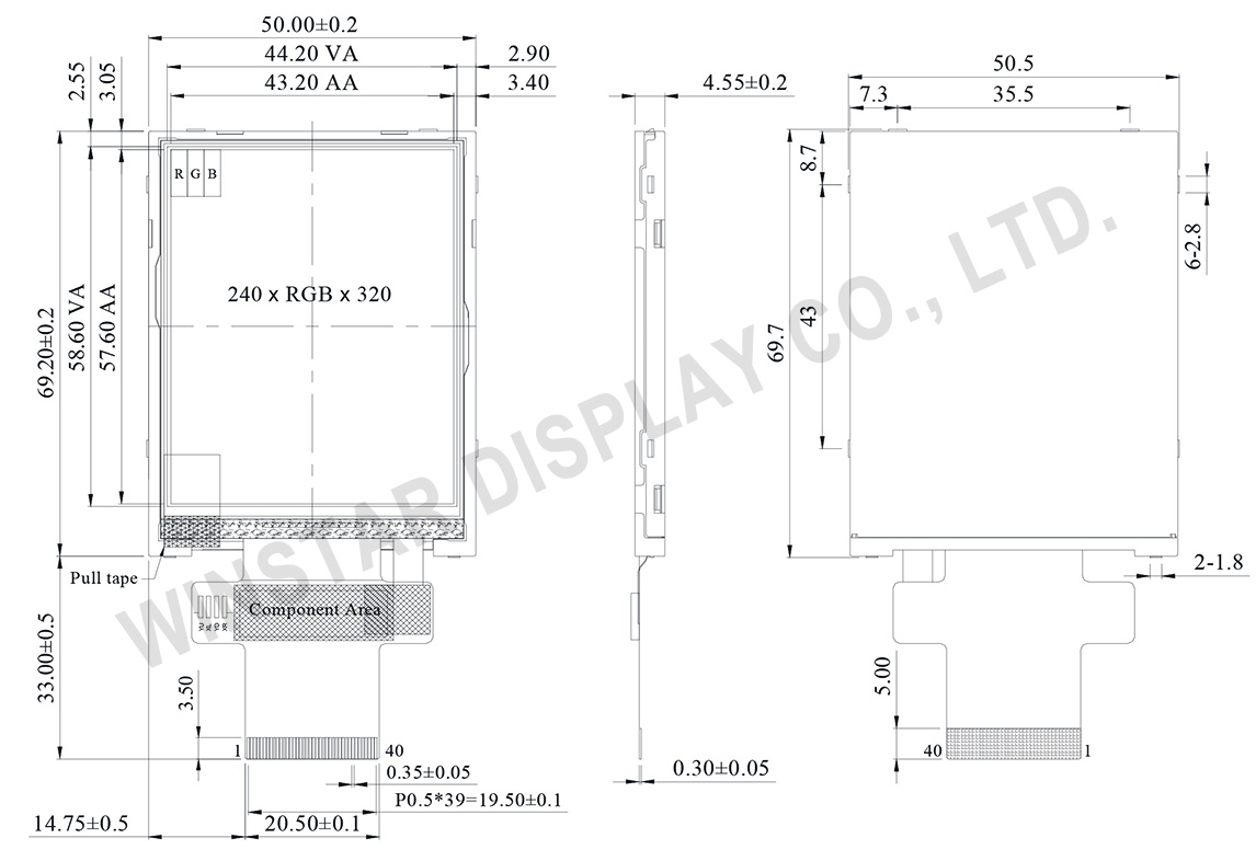
Dimensioni
Unità
Dimensione (Diagonale)
2.8
pollici
A matrice di punti (Risoluzione)
240 x RGB x 320(TFT)
punti
Dimensione del modulo
50.5(W) x 69.7(H) x 4.55(D)
mm
Area attiva
43.2 x 57.6
mm
Passo del Dot
0.18 x 0.18
mm
Tipo LCD
TFT, Nero, Trasmissivo
IC di controllo TFT
ILI9341V o equivalente
Interfaccia TFT
MCU/SPI
Direzione di visione
80/80/80/80
Proporzioni dell’area visiva (ratio)
3:4
Tipo di backlight
LED, Bianco
Touch Screen
senza touch screen
Superficie
Bagliore (Glare)
Valori massimi assoluti
Articolo
Simbolo
Valore Min
Valore tipico
Valore massimo
Unità
Temperatura di lavoro
TOP
-20
-
+70
℃
Temperatura di stock
TST
-30
-
+80
℃
Caratteristiche elettriche
Temperatura di funzionamento
Articolo
Simbolo
Condizione
Valore Min
Valore tipico
Valore massimo
Unità
Supply Voltage for digital
IOVCC
-
1.65
-
3.3
V
Supply Voltage for analog
VCI
-
2.5
-
3.3
V
Power Supply for Current
ICC
IOVCC=VCI
=VCC=3.0V
-
13
20
mA
Condizioni di pilotaggio LED
Parametro
Simbolo
Valore Min
Valore tipico
Valore massimo
Unità
Corrente LED
—
—
100
—
mA
Tensione LED
LEDA
8.1
9.3
10.5
V
Durata LED
—
50000
—
—
Hr
Funzione dei Pin di Interfaccia
Definizione dei Pin LCM
NO
Simbolo
Funzione
I/O
1
GND
Ground
P
2-6
NC
No connection
-
7
VCI
High voltage power supply for analog circuit blocks
(2.5 ~ 3.3 V)
P
8
IOVCC
Low voltage power supply for interface logic circuits
(2.5 ~ 3.3 V)
P
9
TE
Tearing effect output pin to synchronize MPU to frame writing, activated by S/W command. When this pin is not activated, this pin is low.
If not used, open this pin.
O
10
CS
Chip select signal.
I
11
D/CX(SCL)
(D/CX): This pin is used to select “Data or Command” in the parallel interface.
When DCX = 1, data is selected.
When DCX = 0, command is selected.
(SCL): This pin is used as the serial interface clock in 3-wire
9-bit/4-wire 8-bit serial data interface.
If not used, this pin should be connected to IOVCC or GND.
I
12
WR(SPI_D/C)
(WRX) - 8080-Ⅰ/8080-Ⅱ system: Serves as a write signal and writes data at the rising edge.
(D/CX) - 4-line system: Serves as the selector of command or parameter.
Fix to IOVCC level when not in use.
I
13
RD
8080-Ⅰ/8080-Ⅱ system (RDX): Serves as a read signal and MCU read data at the rising edge.
Fix to IOVCC level when not in use.
I
14-29
DB0~DB15
18-bit parallel bi-directional data bus for MCU system.
Fix to GND level when not in use.
I/O
30
RESET
(RESX)This signal will reset the device and must be applied to properly initialize the chip.
Signal is active low.
I
31
IM0
Select the MCU interface mode
IM2
IM1
1M0
MCU-Interface Mode
DB Pin in use
Register/Content
GRAM
0
0
0
80 MCU 8-bit bus interface I
D[7:0]
D[7:0]
0
0
1
80 MCU 16-bit bus interface I
D[7:0]
D[15:0]
0
1
0
80 MCU 9-bit bus interface I
D[7:0]
D[8:0]
0
1
1
80 MCU 18-bit bus interface I
D[7:0]
D[17:0]
1
0
1
3-wire 9-bit data serial interface I
SDA: In/Out
1
1
0
4-wire 8-bit data serial interface I
SDA: In/Out
MPU Parallel interface bus and serial interface select
If use RGB Interface must select serial interface.
* : Fix this pin at IOVCC or GND.
I
32
IM1
33
IM2
34
DB16
18-bit parallel bi-directional data bus for MCU system and RGB
interface mode
Fix to GND level when not in use.
I/O
35
DB17
36
LEDK
Cathode of LED backlight.
P
37
LEDK
Cathode of LED backlight.
P
38
LEDA
Anode of LED backlight.
P
39
SDA
SDA : Serial in/out signal.
The data is applied on the rising edge of the SCL signal.
If not used, fix this pin at IOVCC or GND.
Facendo clic su "Consenti tutti i cookie", accetti la memorizzazione dei cookie sul tuo dispositivo per migliorare la navigazione del sito, analizzare l'utilizzo del sito e assistere nei nostri sforzi di marketing e prestazioni. Puoi trovare ulteriori informazioni su questo argomento nella nostra politica. Informativa sulla privacy