WF28JSYAJDNN0 ist ein 2,8-Zoll IPS TFT LCD-Modul mit einem breiteren Betrachtungswinkel und einer Auflösung von 240x320 Pixeln. Das WF28J-Modul ist im Porträtmodus als IPS TFT-LCD konzipiert und enthält den Controller-IC ILI9341. Es unterstützt MCU-Schnittstellen mit 8-Bit/16-Bit oder SPI und bietet einen Kontrast von 800:1 (typischer Wert). WF28JSYAJDNN0 ist eine High-Brightness-Version mit einer Helligkeit von 1000 Nits (typischer Wert).
Die Versorgungsspannung für die Interface-Logik (IOVCC) des Modells WF28JSYAJDNN0 reicht von 1,65V bis 3,3V, während die Versorgung für den Analogschaltkreis von 2,5V bis 3,3V reicht. Es handelt sich um einen normalerweise schwarzen, transmissiven LCD-Typ mit einem Seitenverhältnis von 3:4 und einer blendenden Glasoberfläche. Der Betriebstemperaturbereich erstreckt sich von -20°C bis +70°C, und die Lagertemperaturen liegen zwischen -30°C und +80°C.
Dieses 2,8-Zoll IPS TFT bietet einen breiteren Betrachtungswinkel als TN TFT, mit Winkeln von Links: 80 / Rechts: 80 / Oben: 80 / Unten: 80 Grad (typischer Wert). IPS-Panels in TFT-Displays bieten einen breiteren Betrachtungswinkel, genaue und konsistente Farbwiedergabe, überragende Bildqualität, präzise Touchscreen-Leistung und eine konstante Farbtemperatur. Die Vielseitigkeit von IPS TFT-LCD-Displays macht sie für verschiedene Anwendungen geeignet, darunter Unterhaltungselektronik, medizinische Displays und industrielle Steuerungspanels.
Zeichnung
Technische Daten
Allgemeine Spezifikationen
Artikel
Ausmaß
Einheit
Größe (Diagonale)
2,8
Zoll
Punktmatrix (Auflösung)
240 x RGB x 320(TFT)
Punkte
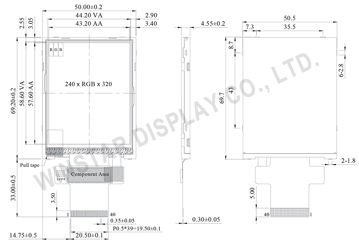
Abmaße der modul
50,5(W) x 69,7(H) x 4,55(D)
mm
Aktiver Bereich
43,2 x 57,6
mm
Punktabstand
0,18 x 0,18
mm
LCD-Typ
TFT, Schwarz, Transmissiv
TFT-Controller-IC
ILI9341V oder gleichwertig
TFT Schnittstelle
MCU/SPI
Blickwinkel
80/80/80/80
Seitenverhältnis
3:4
Backlight-Typ
LED, Weiß
Touchscreen
ohne Touchscreen
Oberfläche
Glanz
absolute Grenzwerte
Artikel
Symbol
Mindestwert
typischer Wert
Maximalwert
Einheit
Betriebstemperatur
TOP
-20
-
+70
℃
Lagertemperatur
TST
-30
-
+80
℃
elektrische Eigenschaften
Betriebsbedingungen
Artikel
Symbol
Bedingung
Mindestwert
typischer Wert
Maximalwert
Einheit
Supply Voltage for digital
IOVCC
-
1,65
-
3,3
V
Supply Voltage for analog
VCI
-
2,5
-
3,3
V
Power Supply for Current
ICC
IOVCC=VCI
=VCC=3.0V
-
13
20
mA
LED-Betriebsbedingungen
Parameter
Symbol
Mindestwert
typischer Wert
Maximalwert
Einheit
LED-Strom
—
—
100
—
mA
LED-Spannung
LEDA
8,1
9,3
10,5
V
LED-Lebensdauer
—
50000
—
—
Hr
Schnittstelle Pin-Funktion
Pinbelegung LCM
NO
Symbol
Funktion
I/O
1
GND
Ground
P
2-6
NC
No connection
-
7
VCI
High voltage power supply for analog circuit blocks
(2.5 ~ 3.3 V)
P
8
IOVCC
Low voltage power supply for interface logic circuits
(2.5 ~ 3.3 V)
P
9
TE
Tearing effect output pin to synchronize MPU to frame writing, activated by S/W command. When this pin is not activated, this pin is low.
If not used, open this pin.
O
10
CS
Chip select signal.
I
11
D/CX(SCL)
(D/CX): This pin is used to select “Data or Command” in the parallel interface.
When DCX = 1, data is selected.
When DCX = 0, command is selected.
(SCL): This pin is used as the serial interface clock in 3-wire
9-bit/4-wire 8-bit serial data interface.
If not used, this pin should be connected to IOVCC or GND.
I
12
WR(SPI_D/C)
(WRX) - 8080-Ⅰ/8080-Ⅱ system: Serves as a write signal and writes data at the rising edge.
(D/CX) - 4-line system: Serves as the selector of command or parameter.
Fix to IOVCC level when not in use.
I
13
RD
8080-Ⅰ/8080-Ⅱ system (RDX): Serves as a read signal and MCU read data at the rising edge.
Fix to IOVCC level when not in use.
I
14-29
DB0~DB15
18-bit parallel bi-directional data bus for MCU system.
Fix to GND level when not in use.
I/O
30
RESET
(RESX)This signal will reset the device and must be applied to properly initialize the chip.
Signal is active low.
I
31
IM0
Select the MCU interface mode
IM2
IM1
1M0
MCU-Interface Mode
DB Pin in use
Register/Content
GRAM
0
0
0
80 MCU 8-bit bus interface I
D[7:0]
D[7:0]
0
0
1
80 MCU 16-bit bus interface I
D[7:0]
D[15:0]
0
1
0
80 MCU 9-bit bus interface I
D[7:0]
D[8:0]
0
1
1
80 MCU 18-bit bus interface I
D[7:0]
D[17:0]
1
0
1
3-wire 9-bit data serial interface I
SDA: In/Out
1
1
0
4-wire 8-bit data serial interface I
SDA: In/Out
MPU Parallel interface bus and serial interface select
If use RGB Interface must select serial interface.
* : Fix this pin at IOVCC or GND.
I
32
IM1
33
IM2
34
DB16
18-bit parallel bi-directional data bus for MCU system and RGB
interface mode
Fix to GND level when not in use.
I/O
35
DB17
36
LEDK
Cathode of LED backlight.
P
37
LEDK
Cathode of LED backlight.
P
38
LEDA
Anode of LED backlight.
P
39
SDA
SDA : Serial in/out signal.
The data is applied on the rising edge of the SCL signal.
If not used, fix this pin at IOVCC or GND.
Durch Klicken auf „Alle Cookies zulassen“ stimmen Sie der Speicherung von Cookies auf Ihrem Gerät zu, um die Navigation auf der Website zu verbessern, die Nutzung der Website zu analysieren und unsere Marketing- und Leistungsbemühungen zu unterstützen. Weitere Informationen zu diesem Thema finden Sie in unserer Richtlinie. Datenschutzrichtlinie