
Startseite Produkte LCD-Display COG LCD WO240128B

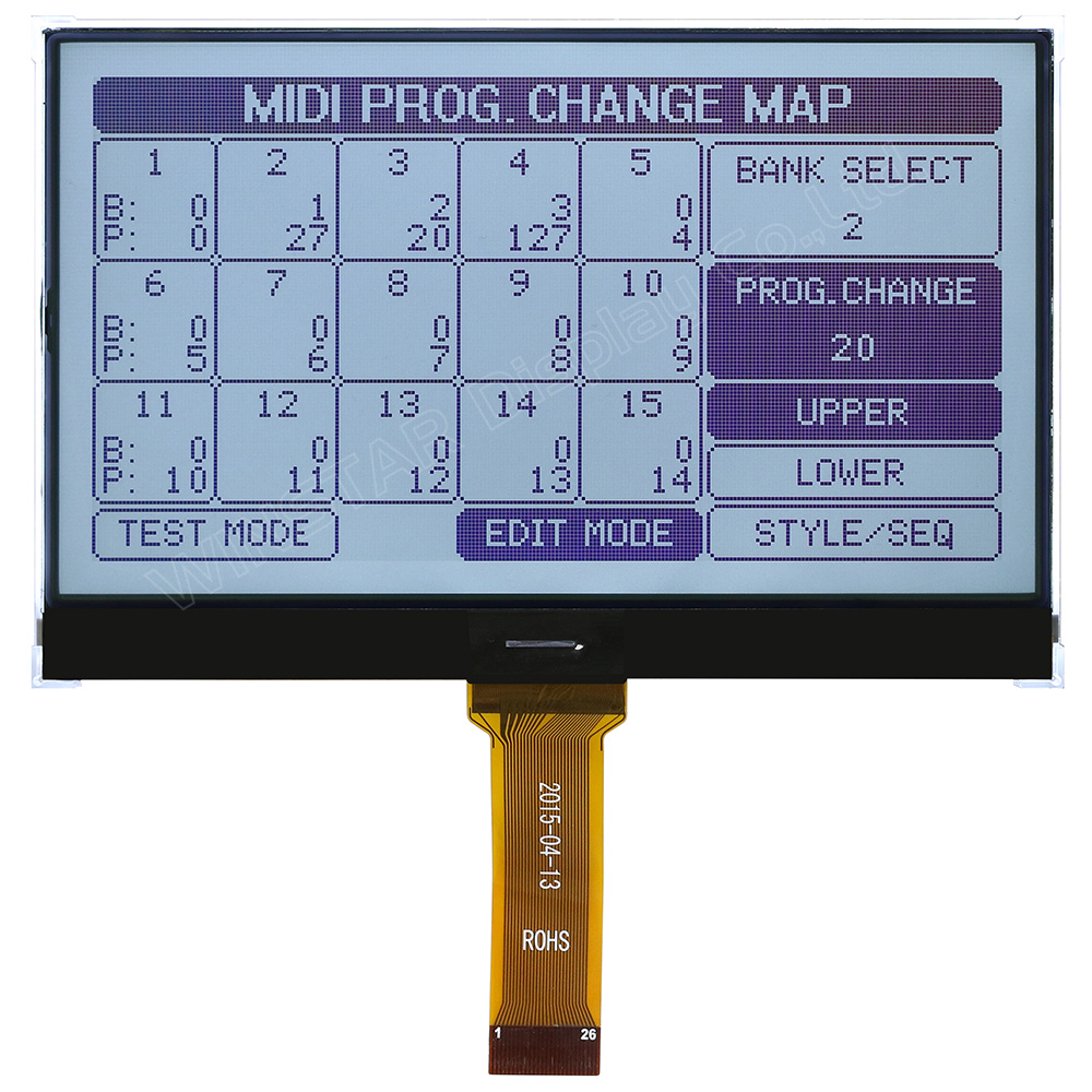
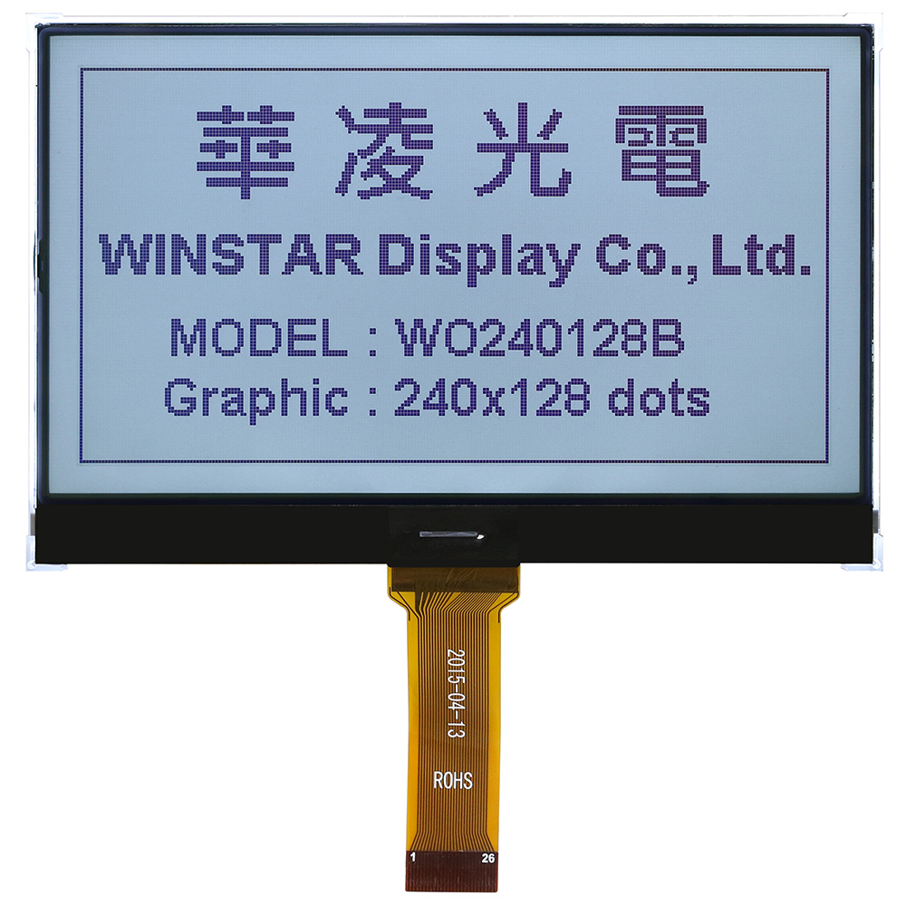
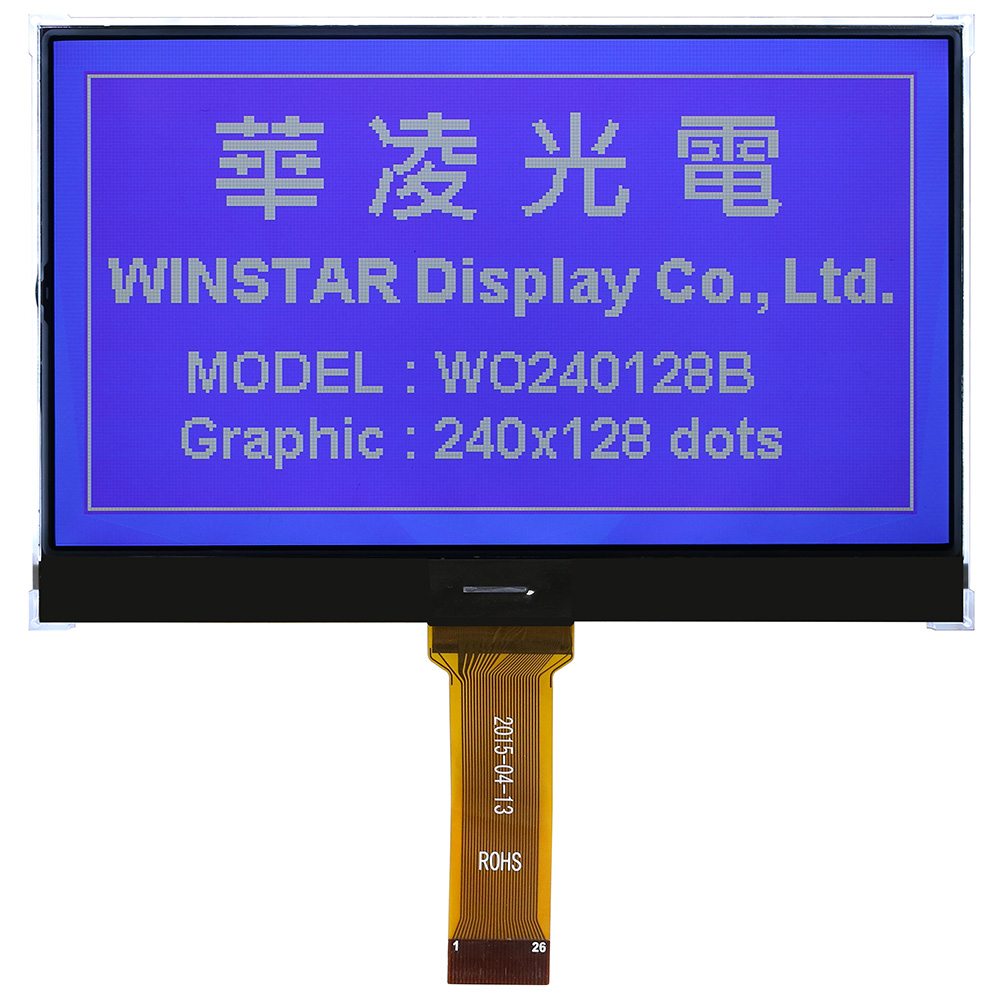
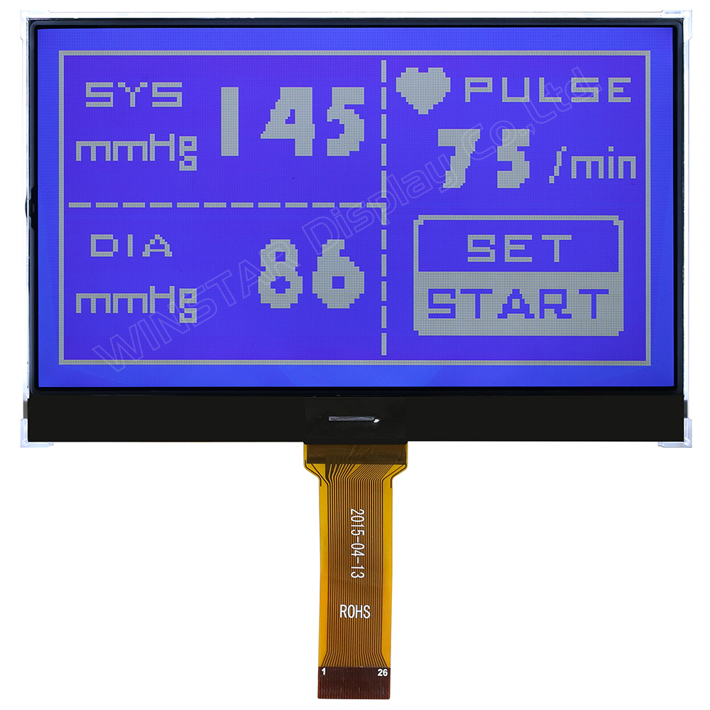
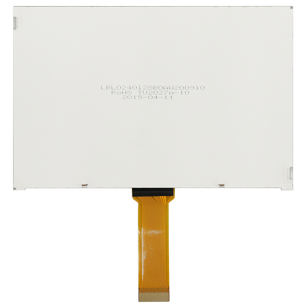
4,82-Zoll grafisches COG-LCD-Modul mit 240x128 Auflösung

Modellnummer WO240128B

►Punktmatrix Display
►Typ: Grafik
►Bauweise: COG
►Größe: 4,82 Zoll
►240x128 Punktmatrix
►IC: ST7586S
►3,3-V-Stromversorgung
►1/128 duty cycle
►Schnittstelle : 6800/8080/SPI

Beschreibung

WO240128B ist ein 4,82-Zoll grafisches COG-LCD-Modul mit 240x128 Auflösung und ST7586S-Controller. Das Modul unterstützt 8-Bit-Parallel-Schnittstellen nach 6800- und 8080-Standard sowie serielle 3-Line- und 4-Line-SPI-Schnittstellen bei einer Logikversorgung von 3,3 V.

Die Modulabmessungen betragen 122,2 x 79,8 x 6,5 mm. Der Sichtbereich misst 114,0 x 64,0 mm, die aktive Anzeigefläche 107,98 x 57,58 mm. Das Modul ist mit einer LED-Hintergrundbeleuchtung ausgestattet.

Im Vergleich zum COB-Modell WG240128B bietet WO240128B bei gleicher Sicht- und Anzeigefläche eine deutlich schlankere COG-Bauweise. Dadurch eignet es sich besonders für Embedded-Systeme, Industrieanlagen und HMI-Anwendungen mit begrenztem Bauraum.

Verschiedene LCD-Ausführungen und LED-Hintergrundbeleuchtungen sind verfügbar. Klicken Sie auf Zur Anfrage hinzufügen und teilen Sie uns Ihre Anforderungen im Anfrageformular mit.

Zeichnung

WO240128B - Contour Drawing

Data source ref:WO240128B-TFH#

Technische Daten

mechanische Daten

Artikel Ausmaß Einheit
Anzahl der Bildpunkte 240 x 128
Module Ausmaß 122.2 x 79.8 x 6.5 (MAX) mm
View area 114.0 x 64.0 mm
Active area 107.98 x 57.58 mm
Dot size 0.43 x 0.43 mm
Dot pitch 0.45 x 0.45 mm
Duty 1/128D,1/12B
Backlight-Typ LED
IC ST7586S
Schnittstelle 6800/8080/3-Line/4-Line

Absolute Maximalwertimum Ratings

Artikel Symbol Mindestwert typischer Wert Maximalwert Einheit
Betriebstemperatur TOP -20 +70
Lagertemperatur TST -30 +80
Digital Power Supply Voltage VDDI -0.3 3.6 V
Analog Power supply voltage VDDA -0.3 3.6 V
LCD Power supply voltage V0-XV0 -0.3 19 V
LCD Power supply voltage VG -0.3 5.5 V

Elektrische Eigenschaften

Artikel Symbol Bedingung Mindestwert typischer Wert Maximalwert Einheit
Supply Voltage For Logic VDD-VSS 3.0 3.3 3.6 V
Supply Voltage For LCM VDD-V0 Ta=-20℃
Ta=25℃
Ta=70℃


14.8


15.0

15.2
V
V
V
Input High Volt. VIH 0.7VDD VDD V
Input Low Volt. VIL VSS 0.3VDD V
Output High Volt. VOH 0.8VDD VDD V
Output Low Volt. VOL VSS 0.2VDD V
Supply Current(No include LED Backlight) IDD VDD=3.3V 2.0 4.0 mA

Schnittstelle Pin-Funktion

Pin No. Symbol Beschreibung
1 ESD GND Electro-Static discharge
2 VG VG is the power of SEG-drivers
3 XV0 Negative operating voltage of COM-drivers
4 V0 Positive operating voltage of COM-drivers
5 VM VM is the non-select voltage level of COM-drivers.
6 VDDA Power supply
7 VSS Ground
8 VD1 Digital power source selection.
9 VDDI VDD1 is the power of interface I/O circuit
10 CSB Chip select input pin
CSB=“L”: This chip is selected and the MPU interface is active
CSB=“H”: This chip is not selected and the MPU interface is disabled
(D[7:0] are high impedance)
11 IF3 These pins select interface operation mode.
IF3 IF2 IF1 MPU interface type
H H L 80 series 8-bit parallel
H L L 68 series 8-bit parallel
L H H 8-bit serial (4-Line)
L H L 9-bit serial (3-Line)
12 IF2
13 IF1
14 RSTB Reset input pin. When RSTB is “L”, internal initialization procedure is executed.
15 /RD(E) Read / Write execution control pin. (This pin is only used in parallel interface)
MPU Type ERD Descriptin
6800-series ERD Read/Write control input pin
R/W = "H" When E is "H", data bus is in output status.
R/W = "L" The data are lunched at the failling edge of the E signal.
8080-series /RD Read enable inputpin.
When /RD is "L". Data bus is in output status.
16~23 D7~D0 The bi-directional data bus of the MPU interface. When CSB is “H”, they are high impedance.
If using serial interface:
D0 is the SDA signal in 4-Line & 3-Line interface.
D1 is the A0 signal in 4-Line interface
24 /WR/(R/W) Read / Write execution control pin. (This pin is only used in parallel interface
MPU Type RWR Descriptin
6800-series R/W Read/Write control input pin
R/W = "H" : Read
R/W = "L" : write
8080-series /WR Write enable clock input pin.
The data are layched at the rising edge of the /WR signal.
This pin is not used in serial interfaces and should be connected to VDD1
25 A0(SCL) The function of this pin is different in parallel and serial interface
In parallel interface: A0 is register selection input
A0 = "H": inputs on data bus are display data
A0 = "L": inputs on data bus are command
In serial interface: this pad will be used as SCL (serial-clock) input
26 ESD GND Electro-Static discharge

Search keyword: 240x128 lcd, 240 x 128 lcd, lcd 240x128, lcd 240 x 128

Ähnliche Produkte

go top
close

Wir schätzen Ihre Privatsphäre

Durch Klicken auf „Alle Cookies zulassen“ stimmen Sie der Speicherung von Cookies auf Ihrem Gerät zu, um die Navigation auf der Website zu verbessern, die Nutzung der Website zu analysieren und unsere Marketing- und Leistungsbemühungen zu unterstützen. Weitere Informationen zu diesem Thema finden Sie in unserer Richtlinie. Datenschutzrichtlinie

Wir schätzen Ihre Privatsphäre

Winstar und bestimmte Drittparteien verwenden Cookies auf www.winstar.com.tw. Die Einzelheiten zu den Arten von Cookies, ihrem Zweck und den beteiligten Drittparteien sind unten sowie in unserer Cookie-Richtlinie beschrieben. Klicken Sie auf „Alle zulassen“, um unserer Verwendung von Cookies zuzustimmen und die bestmögliche Erfahrung auf unseren Websites zu erzielen. Sie können auch Ihre Präferenzen festlegen oder Cookies ablehnen (mit Ausnahme der unbedingt erforderlichen Cookies).

Einwilligungspräferenzen verwalten

Immer aktiv
Notwendige Cookies

Diese Cookies sind unerlässlich, um Ihnen das Navigieren auf der Website zu ermöglichen und ihre Funktionen zu nutzen, wie z. B. das Festlegen Ihrer Datenschutzpräferenzen, das Einloggen oder das Ausfüllen von Formularen.

Analyse-Cookies

Diese Cookies, auch als „Statistik-Cookies“ bekannt, sammeln Informationen darüber, wie Sie eine Website nutzen, z. B. welche Seiten Sie besucht und auf welche Links Sie geklickt haben. Siehe Details.