
PMOLED Compatible Solution for SSD1307 and CH1115 IC
Since SSD1307 is going to be EOL, we developed a new series of products using CH1115 instead of SSD1307. When developing products, we keep the original module design as much as possible so the modules of SSD1307 and CH1115 are compatible with each other.
The following will explain the differences between the two models from the hardware and software perspective and how to achieve compatibility.
| Related Module Series | |
|---|---|
| Past model(SSD1307) | New model(CH1115) |
| WEO012832G | WEO012832P |
1. Hardware
Some pins of SSD1307 and CH1115 have different names but the same functions. For example, VCC, D/C, and BS0 of SSD1307 are equivalent to VPP, A0, and IM0 of CH1115. Although some pins have the same function, different passive components need to be selected, such as the resistor of the IREF pin. The recommended circuit diagrams of the two ICs are shown in Figure 1 and Figure 2.
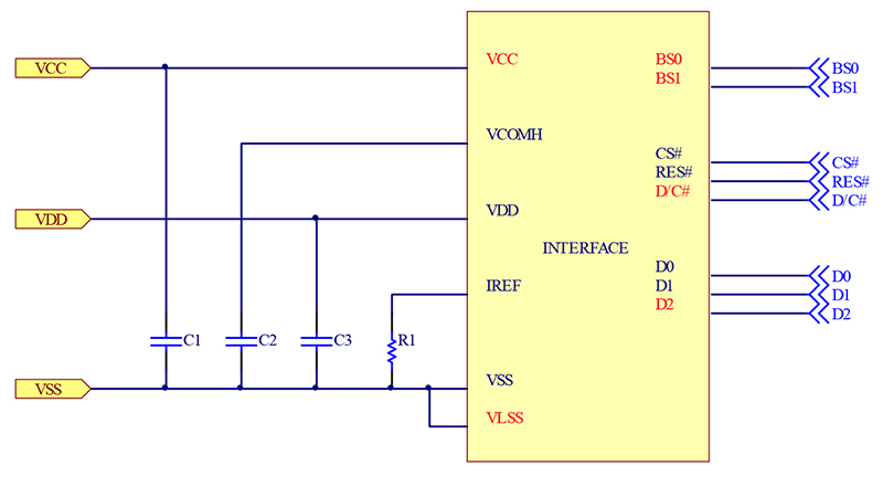
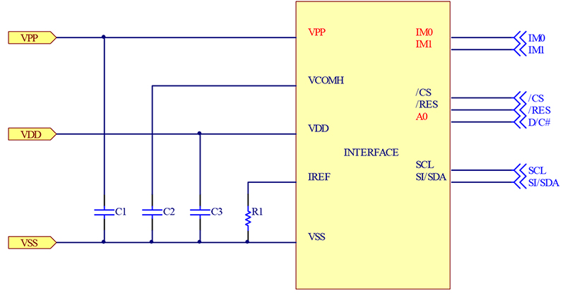
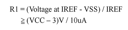
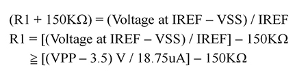
Please pay attention to the resistance value of pin IREF, which can directly affect the brightness and current. When both ICs use the same VCC (VPP), the SSD1307 needs a larger resistance value. The formula for the resistance is below.
SSD1307:
CH1115:
2. Software
Most of the commands of SSD1307 and CH1115 are compatible, but some are still different. For example, two ICs each have exclusive functions, so the IC can only use some commands. In addition, some commands have the same function, but the parameters are incompatible, as shown in Table 2.
| SSD1307 | CH1115 | |
|---|---|---|
| Set Memory Addressing Mode 20H |
Set the way of memory addressing into one of the below three modes. 00H:Horizontal Addressing Mode 01H:Vertical Addressing Mode 02H:Page Addressing Mode |
N/A |
| Set Pump voltage value 30H~33H |
N/A | Specifies output voltage (VPP) of the internal charger pump. 30H: 10V;31H: 7.4V;32H: 8V;33H: 9V |
| Set Display Start Line 40H~66H/7FH |
Sets the Display Start Line register to determine starting address of display RAM. (40H~66H) |
Specifies RAM display line for COM0. (40H~7FH) |
| IREF Resistor Set 82H |
N/A | IREF can be controlled by external resister or internal resister. |
| Set Segment Re-map A0H~A1H |
N/A | Change the relationship between RAM column address and segment driver. |
| Set SEG pads hardware configuration A2H~A3H |
N/A | Set the SEG signals pad configuration to match the OLED panel hardware layout. |
| Set DC-DC OFF/ON ADH |
N/A | This command is to control the DC-DC voltage converter. |
| Set Display Offset D3H |
This is a double byte command which specifies the mapping of the display start line to one of COM0~COM38. | This is a double byte command which specifies the mapping of display start line to one of COM0~COM63. |
| Set Display Clock Divide Ratio/Oscillator Frequency D5H |
Dicide Ratio:1~16 | Dicide Ratio:3、4、8、16 |
| Set Pre-charge Period D9H |
A[3:0]:Dis-charge A[7:4]:Pre-charge |
A[3:0]:Pre-charge A[7:4]:Dis-charge |
| Set COM Pins Hardware Configuration DAH |
02H:Sequential Mode; Disable COM Left/Right remap 12H:Alternative Mode; Disable COM Left/Right remap 22H:Sequential Mode; Enable COM Left/Right remap 32H:Alternative Mode; Enable COM Left/Right remap |
N/A |
| Set VCOMH Deselect Level DBH |
00H:0.65 x VCC 20H:0.77 x VCC 30H:0.83 x VCC |
00H:0.430 x VCC ~ 40H:VCC |
| Set row non-overlap/SEG Hiz Period DCH |
N/A | This command is used to set the duration of the row non-overlap /SEG Hiz Period period. |
| Set Command Lock FDH |
Set Command Lock | N/A |
3. Compatibility
In order to make the ICs compatible with each other, the hardware and software of the module need to be modified.
The pins of the two ICs are roughly the same in terms of hardware. The resistance value of IREF must conform to the respective calculation formulas at the same time. If the resistance value is too small, there is a risk of burning out the IC. In addition, VCC (VPP) must follow the specifications of SSD1307 and CH1115 simultaneously; the former is 7V~16V, and the latter is 6.4V~14V.
In terms of software, there are three points to note:
1.There are many Memory Addressing Modes for SSD1307, but CH1115 only has Page Addressing Mode. Therefore, we recommend using Page Addressing Mode.
2.The resolution of the SSD1307 supports 128x39, and that of the CH1115 is 128x64. This difference makes the layout of the panel different. Therefore, when setting Display Offset (D3h) and Segment Remap (A0h/A1h), we should avoid pattern offset caused by different start addresses.
3. We can choose whether to turn on the DC-DC Voltage Converter (ADh) of CH1115, but SSD1307 does not have this function. We recommend turning off the DC-DC converter of CH1115 and using external VCC/VPP.
In addition, by setting the Command Lock (FDh) of SSD1307, the respective commands of the two ICs can be written in the same initial code. After using FDh to lock the IC, SSD1307 accepts no commands except FDh, but CH1115 is unaffected. Therefore, we can issue commands to the two ICs separately.
4. Conclusion
These two ICs, SSD1307 and CH1115, are compatible with each other. We can display the same image and brightness using the same hardware and software. As long as the components, such as resistors and capacitors, are adjusted and the initial code is modified, SSD1307 can be replaced with CH1115. According to the situation, we can modify the software slightly without changing the hardware to make the two ICs achieve the same display effect.
We will continue to provide high-quality products and competitive solutions.
