


製品情報
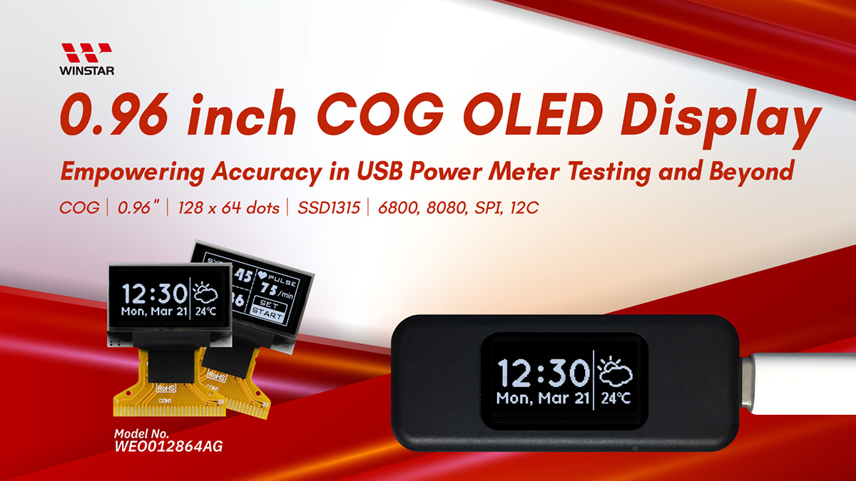
WEO012864AGは、モノクロパッシブマトリックス、グラフィックCOG(Chip-on- Glass)構造を採用し、対角寸法は0.96インチ、128x64の解像度と10000:1の高コントラスト比を持っているOLEDモジュールです。ロジック電源電圧は3V、デューティ比は1/64です。WEO012864AGシリーズはSSD1315 ICを搭載して、8ビット6800/8080、I2C、3線/4線SPIインタフェースをサポートし、内部電源電圧と外部電源の選択ができます。
この OLED モジュールの動作温度は-30℃ ~+70℃で、保管温度は-30℃ ~ +70℃です。 多用途に考慮して設計され、特に医療設備を向いています。例え:血中酸素濃度測定器や各種の測定機器。 USB 電源検査装置、デジタル角度計などの設備でも適用します。
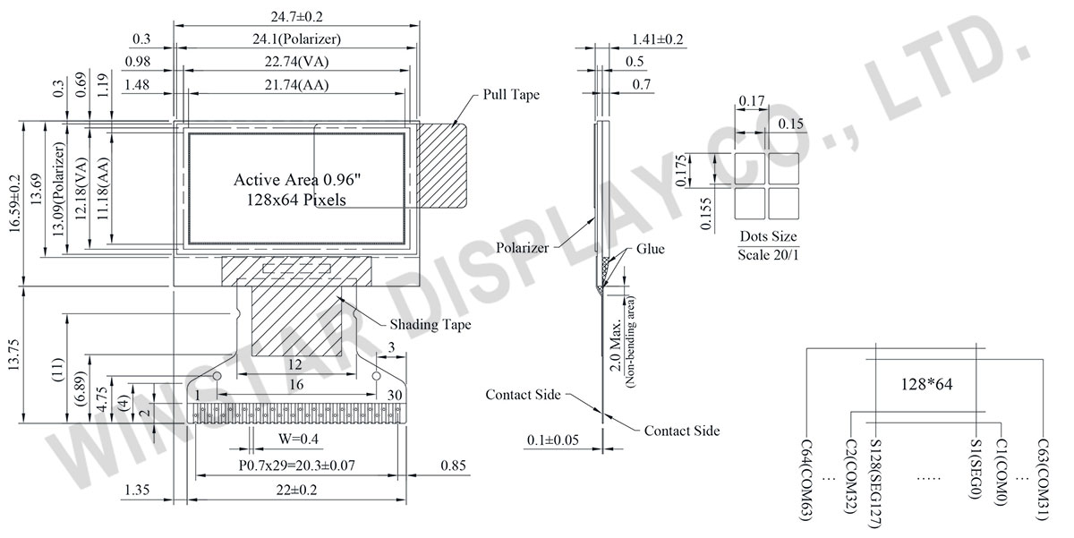
外形図
Data source ref:WEO012864AGWPP3N0Y000
製品仕様
ピン功能定義
| Pin No. | 記号 | 功能 | ||||||||||||||||||||||||
|---|---|---|---|---|---|---|---|---|---|---|---|---|---|---|---|---|---|---|---|---|---|---|---|---|---|---|
| 1 | N.C. (GND) | The supporting pins can reduce the influences from stresses on the function pins. These pins must be connected to external ground. | ||||||||||||||||||||||||
| 2 | C2P | C1P/C1N – Pin for charge pump capacitor; Connect to each other with a capacitor. C2P/C2N – Pin for charge pump capacitor; Connect to each other with a capacitor. |
||||||||||||||||||||||||
| 3 | C2N | |||||||||||||||||||||||||
| 4 | C1P | |||||||||||||||||||||||||
| 5 | C1N | |||||||||||||||||||||||||
| 6 | VBAT | This is the power supply pin for the internal buffer of the DC/DC voltage converter. It must be connected to external source when the converter is used. It should be connected to VDD when the converter is not used. | ||||||||||||||||||||||||
| 7 | NC | NC | ||||||||||||||||||||||||
| 8 | VSS | This is a ground pin. | ||||||||||||||||||||||||
| 9 | VDD | Power supply pin for core logic operation. | ||||||||||||||||||||||||
| 10 | BS0 | These pins are MCU interface selection input. See the following table:
|
||||||||||||||||||||||||
| 11 | BS1 | |||||||||||||||||||||||||
| 12 | BS2 | |||||||||||||||||||||||||
| 13 | CS# | This pin is the chip select input connecting to the MCU. The chip is enabled for MCU communication only when CS# is pulled LOW (active LOW). |
||||||||||||||||||||||||
| 14 | RES# | This pin is reset signal input. When the pin is low, initialization of the chip is executed. Keep this pin HIGH (i.e. connect to VDD) during normal operation. | ||||||||||||||||||||||||
| 15 | D/C# | This pin is Data/Command control pin connecting to the MCU. When the pin is pulled HIGH, the data at D[7:0] will be interpreted as data. When the pin is pulled LOW, the data at D[7:0] will be transferred to a command register. In I2C mode, this pin acts as SA0 for slave address selection. When 3-wire serial interface is selected, this pin must be connected to VSS. |
||||||||||||||||||||||||
| 16 | R/W# | This is read / write control input pin connecting to the MCU interface. When interfacing to a 6800-series microprocessor, this pin will be used as Read/Write (R/W#) selection input. Read mode will be carried out when this pin is pulled HIGH (i.e. connect to VDD) and write mode when LOW. When 8080 interface mode is selected, this pin will be the Write (WR#) input. Data write operation is initiated when this pin is pulled LOW and the chip is selected. When serial or I2C interface is selected, this pin must be connected to VSS. |
||||||||||||||||||||||||
| 17 | E/RD# | This pin is MCU interface input. When 6800 interface mode is selected, this pin will be used as the Enable (E) signal. Read/write operation is initiated when this pin is pulled HIGH and the chip is selected. When 8080 interface mode is selected, this pin receives the Read (RD#) signal. Read operation is initiated when this pin is pulled LOW and the chip is selected. When serial or I2C interface is selected, this pin must be connected to VSS. |
||||||||||||||||||||||||
| 18~25 | D0~D7 | These pins are bi-directional data bus connecting to the MCU data bus. Unused pins are recommended to tie LOW. When serial interface mode is selected, D2 should be either tied LOW or tied together with D1 as the serial data input: SDIN, and D0 will be the serial clock input: SCLK. When I2C mode is selected, D2, D1 should be tied together and serve as SDAout, SDAin in application and D0 is the serial clock input, SCL. |
||||||||||||||||||||||||
| 26 | IREF | When external IREF is used, a resistor should be connected between this pin and VSS to maintain the IREF current at a maximum of 30uA. When internal IREF is used, this pin should be kept NC. |
||||||||||||||||||||||||
| 27 | VCOMH | COM signal deselected voltage level. A capacitor should be connected between this pin and VSS. |
||||||||||||||||||||||||
| 28 | VCC | Power supply for panel driving voltage. This is also the most positive power voltage supply pin. When charge pump is enabled, a capacitor should be connected between this pin and VSS. |
||||||||||||||||||||||||
| 29 | VLSS | This is an analog ground pin. It should be connected to VSS externally. | ||||||||||||||||||||||||
| 30 | NC (GND) |
The supporting pins can reduce the influences from stresses on the function pins. These pins must be connected to external ground. |
規格説明
| 項目 | 標準値 | 単位 |
|---|---|---|
| ドットマトリックス(解像度) | 128 x 64 | - |
| モジュールサイズ | 24.7 x 16.59 x 1.41 | mm |
| 有効エリア | 21.74 x 11.18 | mm |
| ドットサイズ | 0.15 x 0.155 | mm |
| ドットピッチ | 0.17 x 0.175 | mm |
| 表示モード | パッシブマトリクス | |
| 発光色 | モノクロ | |
| 駆動方法 | 1/64 Duty | |
| IC | SSD1315 | |
| インターフェース | 6800,8080,SPI,I2C | |
| 表示サイズ(対角線) | 0.96 インチ | |
絶対最大定格
| パラメーター | 記号 | 最小値 | 最大値 | 単位 |
|---|---|---|---|---|
| ロジック電源電圧 | VDD | 0 | 4 | V |
| Charge Pump Regulator Supply Voltage | VBAT | -0.3 | 6.0 | V |
| Display電源電圧 | VCC | 0 | 18.0 | V |
| 操作温度 | TOP | -30 | +70 | ℃ |
| 保存温度 | TSTG | -30 | +70 | ℃ |
電気特性
| 項目 | 記号 | 条件 | 最小値 | 典型値 | 最大値 | 単位 |
|---|---|---|---|---|---|---|
| ロジック電源電圧 | VDD | - | 1.65 | 3.0 | 3.3 | V |
| Display電源電圧(Supplied Externally) | VCC | - | 7.5 | - | 8.0 | V |
| Charge Pump Regulator Supply Voltage | VBAT | - | 3.0 | 3.5 | 4.5 | V |
| Charge Pump Output Voltage for Display (Generated by Internal DC/DC) | Charge Pump VCC | - | 7.0 | 7.5 | - | V |
| 高レベル入力電圧 | VIH | - | 0.8xVDD | - | - | V |
| 低レベル入力電圧 | VIL | - | - | - | 0.2VDD | V |
| 高レベル出力電圧 | VOH | - | 0.9xVDD | - | - | V |
| 低レベル出力電圧 | VOL | - | - | - | 0.1xVDD | V |
| Operating Current for VCC (Display 50% Pixel on)(VCC Supplied Externally) |
ICC | VCC=7.5V | - | 5.0 | 10 | mA |
| Display 50% Pixel on (VCC Generated by Internal DC/DC) |
IBAT | VBAT=3.5V | - | 15 | 22.5 | mA |
Search keyword: 128x64 lcd, 128 x 64 lcd, lcd 128x64, lcd 128 x 64

