


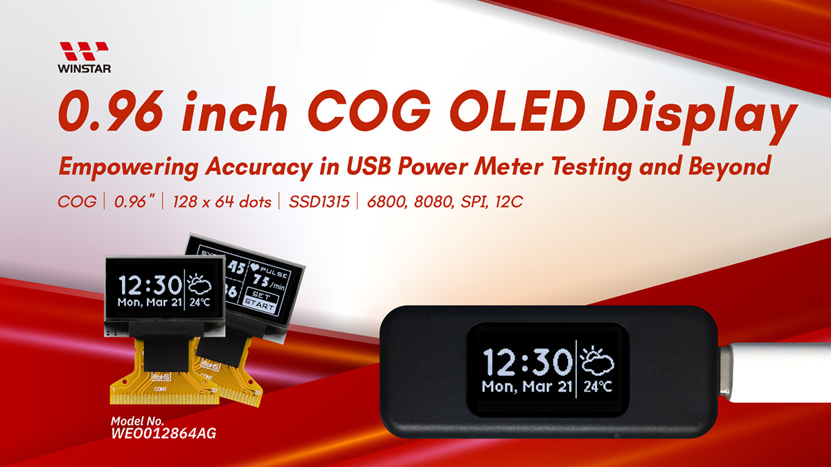
128x64 0.96 дюймовый монохромный OLED дисплейный модуль
Артикул. WEO012864AG
►Тип: Графический
►Тип монтажа контроллера: COG
►Диагональ: 0.96 дюйма
►Разрешение: 128 x 64 точек
►IC:SSD1315
►3V Power supply
►1/64 duty
►Интерфейс: 6800, 8080, SPI, I2C
►Цвет дисплея: Белый
Описание
WEO012864AG – это серия 0.96-дюймовых COG OLED-дисплеев с разрешением 128x64 точек. Дисплей работает на базе контроллера IC SSD1315, поддерживающего параллельные интерфейсы 6800/8080, I2C и SPI. Напряжение питания для логики дисплея составляет 3 V (типичное значение), а напряжение питания для дисплея – 18V (максимальное значение) с рабочим циклом 1/64. Этот OLED-индикатор обладает высоким контрастом - 10,000:1 (типичное значение), что обеспечивает четкое отображение информации. Шлейф дисплея предназначен для прямого монтажа на печатную плату посредством пайки.
WEO012864AG может работать при температурах от -30 ° С до + 70 ℃, а температура хранения составляет от -30 ℃ до + 70 ℃.
OLED-дисплеи серии WEO012864AG идеально подходят для портативных измерительных приборов, умных счетчиков, устройств IoT, благодаря толщине (1.41 мм), малому весу и низкому энергопотреблению.
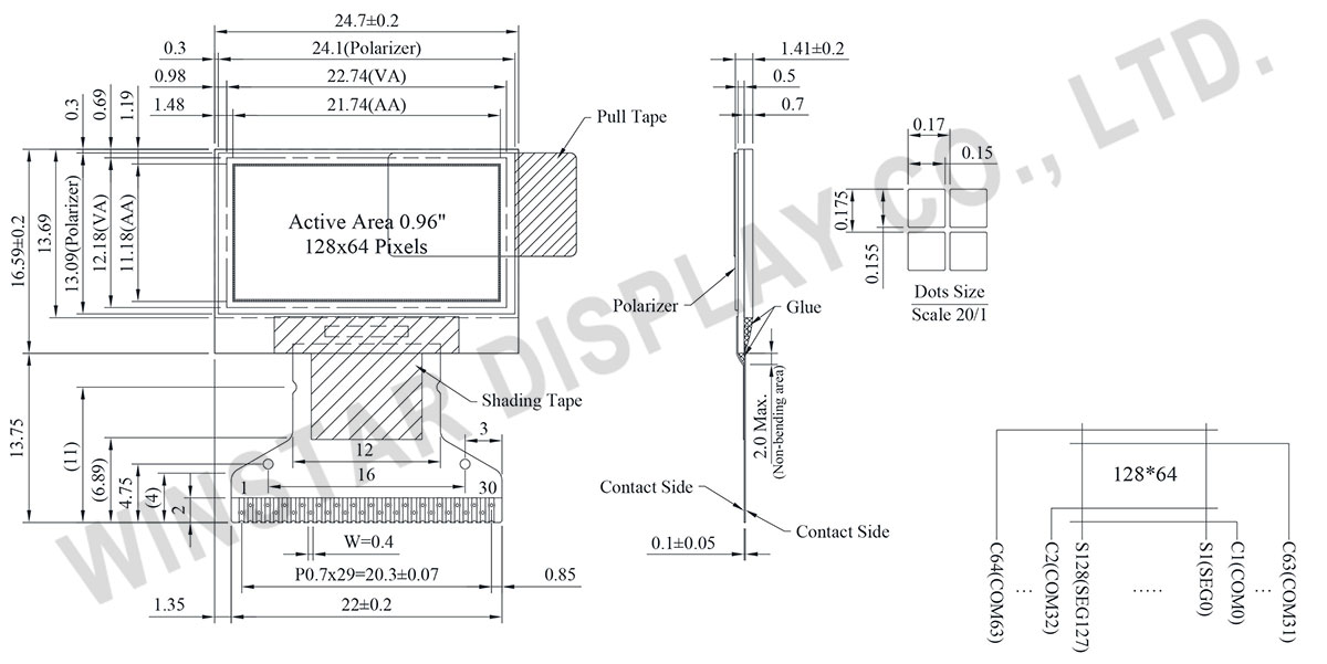
Чертеж
Технические характеристики
Функции контроллера контактного интерфейса
| Pin No. | Символы | Описание | ||||||||||||||||||||||||
|---|---|---|---|---|---|---|---|---|---|---|---|---|---|---|---|---|---|---|---|---|---|---|---|---|---|---|
| 1 | N.C. (GND) | The supporting pins can reduce the influences from stresses on the function pins. These pins must be connected to external ground. | ||||||||||||||||||||||||
| 2 | C2P | C1P/C1N – Pin for charge pump capacitor; Connect to each other with a capacitor. C2P/C2N – Pin for charge pump capacitor; Connect to each other with a capacitor. |
||||||||||||||||||||||||
| 3 | C2N | |||||||||||||||||||||||||
| 4 | C1P | |||||||||||||||||||||||||
| 5 | C1N | |||||||||||||||||||||||||
| 6 | VBAT | This is the power supply pin for the internal buffer of the DC/DC voltage converter. It must be connected to external source when the converter is used. It should be connected to VDD when the converter is not used. | ||||||||||||||||||||||||
| 7 | NC | NC | ||||||||||||||||||||||||
| 8 | VSS | This is a ground pin. | ||||||||||||||||||||||||
| 9 | VDD | Power supply pin for core logic operation. | ||||||||||||||||||||||||
| 10 | BS0 | These pins are MCU interface selection input. See the following table:
|
||||||||||||||||||||||||
| 11 | BS1 | |||||||||||||||||||||||||
| 12 | BS2 | |||||||||||||||||||||||||
| 13 | CS# | This pin is the chip select input connecting to the MCU. The chip is enabled for MCU communication only when CS# is pulled LOW (active LOW). |
||||||||||||||||||||||||
| 14 | RES# | This pin is reset signal input. When the pin is low, initialization of the chip is executed. Keep this pin HIGH (i.e. connect to VDD) during normal operation. | ||||||||||||||||||||||||
| 15 | D/C# | This pin is Data/Command control pin connecting to the MCU. When the pin is pulled HIGH, the data at D[7:0] will be interpreted as data. When the pin is pulled LOW, the data at D[7:0] will be transferred to a command register. In I2C mode, this pin acts as SA0 for slave address selection. When 3-wire serial interface is selected, this pin must be connected to VSS. |
||||||||||||||||||||||||
| 16 | R/W# | This is read / write control input pin connecting to the MCU interface. When interfacing to a 6800-series microprocessor, this pin will be used as Read/Write (R/W#) selection input. Read mode will be carried out when this pin is pulled HIGH (i.e. connect to VDD) and write mode when LOW. When 8080 interface mode is selected, this pin will be the Write (WR#) input. Data write operation is initiated when this pin is pulled LOW and the chip is selected. When serial or I2C interface is selected, this pin must be connected to VSS. |
||||||||||||||||||||||||
| 17 | E/RD# | This pin is MCU interface input. When 6800 interface mode is selected, this pin will be used as the Enable (E) signal. Read/write operation is initiated when this pin is pulled HIGH and the chip is selected. When 8080 interface mode is selected, this pin receives the Read (RD#) signal. Read operation is initiated when this pin is pulled LOW and the chip is selected. When serial or I2C interface is selected, this pin must be connected to VSS. |
||||||||||||||||||||||||
| 18~25 | D0~D7 | These pins are bi-directional data bus connecting to the MCU data bus. Unused pins are recommended to tie LOW. When serial interface mode is selected, D2 should be either tied LOW or tied together with D1 as the serial data input: SDIN, and D0 will be the serial clock input: SCLK. When I2C mode is selected, D2, D1 should be tied together and serve as SDAout, SDAin in application and D0 is the serial clock input, SCL. |
||||||||||||||||||||||||
| 26 | IREF | When external IREF is used, a resistor should be connected between this pin and VSS to maintain the IREF current at a maximum of 30uA. When internal IREF is used, this pin should be kept NC. |
||||||||||||||||||||||||
| 27 | VCOMH | COM signal deselected voltage level. A capacitor should be connected between this pin and VSS. |
||||||||||||||||||||||||
| 28 | VCC | Power supply for panel driving voltage. This is also the most positive power voltage supply pin. When charge pump is enabled, a capacitor should be connected between this pin and VSS. |
||||||||||||||||||||||||
| 29 | VLSS | This is an analog ground pin. It should be connected to VSS externally. | ||||||||||||||||||||||||
| 30 | NC (GND) |
The supporting pins can reduce the influences from stresses on the function pins. These pins must be connected to external ground. |
Механические характеристики
| Наименование | Измерения | Единица |
|---|---|---|
| Разрешение | 128 x 64 | - |
| Габариты | 24.7 x 16.59 x 1.41 | mm |
| Активная область | 21.74 x 11.18 | mm |
| Размер пикселя | 0.15 x 0.155 | mm |
| Шаг пикселя | 0.17 x 0.175 | mm |
| Матрица | Пассивная | |
| Цвет дисплея | монохромные | |
| Рабочий цикл | 1/64 Duty | |
| IC | SSD1315 | |
| Интерфейс | 6800,8080,SPI,I2C | |
| Диагональ | 0.96 Дюйм | |
Абсолютные максимальные значения
| Параметр | Символы | Минимальный | Максимальный | Единица |
|---|---|---|---|---|
| Напряжение питания логических схем | VDD | 0 | 4 | V |
| Charge Pump Regulator Supply Voltage | VBAT | -0.3 | 6.0 | V |
| Напряжение питания дисплея | VCC | 0 | 18.0 | V |
| Диапазон рабочих температур | TOP | -30 | +70 | ℃ |
| Температура хранения | TSTG | -30 | +70 | ℃ |
Электронные характеристики
| Наименование | Символы | Condition | Минимальный | Типичный | Максимальный | Единица |
|---|---|---|---|---|---|---|
| Напряжение питания логических схем | VDD | - | 1.65 | 3.0 | 3.3 | V |
| Напряжение питания дисплея (Supplied Externally) |
VCC | - | 7.5 | - | 8.0 | V |
| Charge Pump Regulator Supply Voltage | VBAT | - | 3.0 | 3.5 | 4.5 | V |
| Charge Pump Output Voltage for Display (Generated by Internal DC/DC) | Charge Pump VCC | - | 7.0 | 7.5 | - | V |
| Высокое входное напряжение | VIH | - | 0.8xVDD | - | - | V |
| Низкое входное напряжение | VIL | - | - | - | 0.2VDD | V |
| Output High Volt. | VOH | - | 0.9xVDD | - | - | V |
| Output Low Volt. | VOL | - | - | - | 0.1xVDD | V |
| Operating Current for VCC (Display 50% Pixel on)(VCC Supplied Externally) |
ICC | VCC=7.5V | - | 5.0 | 10 | mA |
| Display 50% Pixel on (VCC Generated by Internal DC/DC) |
IBAT | VBAT=3.5V | - | 15 | 22.5 | mA |
Search keyword: 128x64 lcd, 128 x 64 lcd, lcd 128x64, lcd 128 x 64
