
 - WL0F00043000WGAAASA00")

우리는 귀하의 프라이버시를 소중히 여깁니다
"모든 쿠키 허용"을 클릭하면 사이트 탐색을 개선하고, 사이트 사용을 분석하며, 마케팅 및 성능 노력에 도움을 주기 위해 쿠키를 귀하의 장치에 저장하는 데 동의한 것으로 간주됩니다. 이 주제에 대한 추가 정보는 당사의 정책에서 확인할 수 있습니다. 개인정보 보호정책


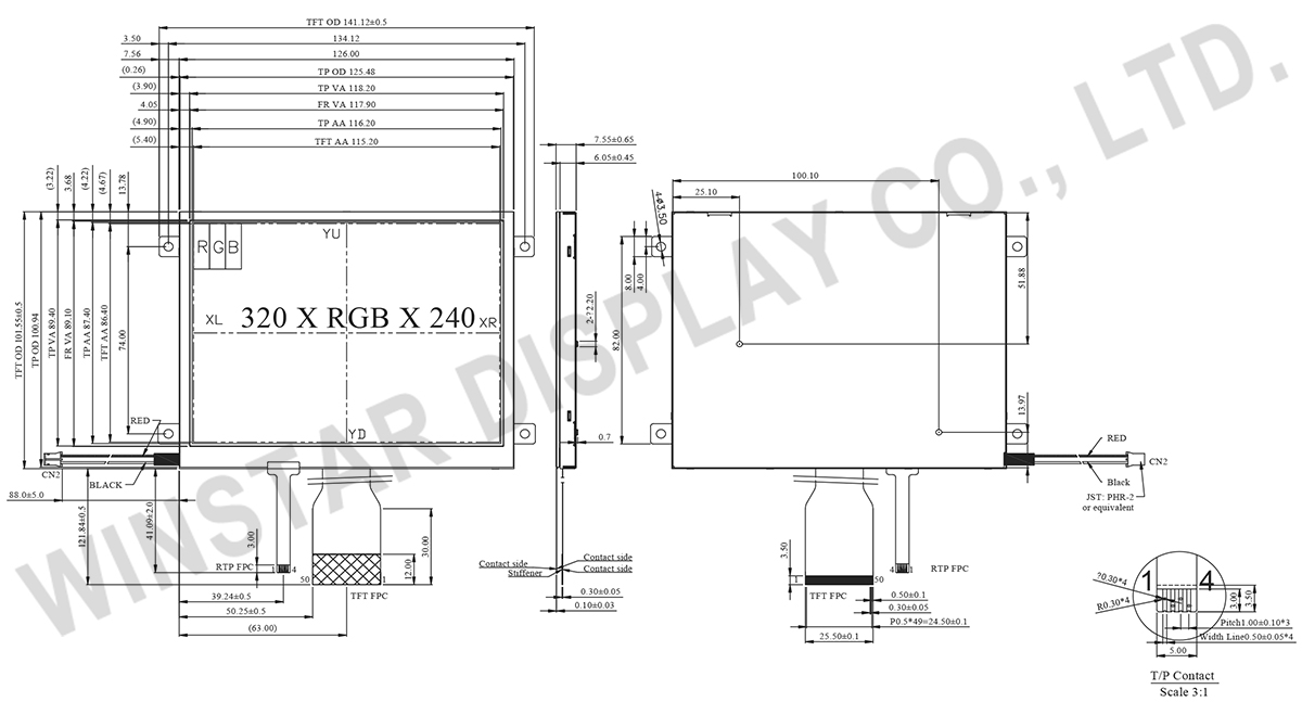
WF57ZTIGCDNT0는 다양한 산업 요구를 충족시키기 위해 설계된 5.7인치 표준 TFT LCD 디스플레이 모듈입니다. 해상도는 320x240 픽셀이며 종횡비는 4:3으로, 이 모듈은 다양한 응용 분야에 명확한 시각을 제공합니다. 모듈 크기는 141.12 × 101.55 mm이며, 활성 영역은 115.2 × 86.40 mm이며, 4개의 나사 구멍과 금속 프레임이 장착되어 설치가 신속하고 안전합니다.
반사가 최소화되어 우수한 이미지 품질을 보장하는 안티글레어 디스플레이 표면 덕분에, 화면의 작동 온도는 -20℃에서 +70℃까지이며, 저장 온도는 -30℃에서 +80℃까지 범위합니다. 전압 공급 범위가 3.2V에서 3.4V이며, 전형적인 값은 3.3V인 이 TFT 디스플레이 모듈은 HX8218 및 HX8615 드라이버 IC를 특징으로 하며, 24비트 RGB 인터페이스를 지원합니다. 밝기는 600 cd/m²이고 대조 비율 (전형적인 값)은 300:1로, 반사가 최소화되어 우수한 이미지 품질을 보장합니다.
주요 응용 분야:
산업 제어 패널: 공장, 생산 라인 및 기계의 제어 패널에 적합합니다.
내비게이션 장치: 명확한 내비게이션 맵을 제공하는 GPS 장치 및 해양 차트 플로터에 이상적입니다.
믹싱 콘솔: 스튜디오, 콘서트 장소 및 방송 시설에서 전문적인 오디오 믹싱에 완벽합니다.
의료 모니터링 장비: 병원 및 클리닉의 혈압 모니터 및 생리학 모니터에 적합합니다.
소매 POS 시스템: 제품 정보와 거래 내역을 표시하는 POS 시스템에 적합합니다.
홈 오토메이션 패널: 스마트 홈 장치의 모니터링 및 제어를 쉽게 할 수 있습니다.
| 항목 | 치수 | 단위 |
|---|---|---|
| 크기 | 5.7 | 인치 |
| 도트 매트릭스 | 320 × RGB × 240 (TFT) | dots |
| 모듈 치수 | 141.12(W) × 101.55(H) ×7.55 (D) | mm |
| 활성 영역 | 115.2 × 86.40 | mm |
| 도트 피치 | 0.12 × 0.36 | mm |
| LCD 유형 | TFT, 백색, 투과성 | |
| 뷰 방향 | 12 o'clock | |
| 그레이스케일 반전 방향 | 6 o'clock | |
| TFT 드라이버 IC | HX8218+HX8615 또는 이와 동등한 | |
| 인터페이스 | 24-bit RGB | |
| 종횡비 | 4:3 | |
| 역광 타입 | LED, 백색 | |
| 터치 패널 포함/제외 | 저항식 터치패널이 있는 (RTP) | |
| 표면 | 눈부심 방지 | |
| 항목 | 기호 | 최소값 | 대표값 | 최대값 | 단위 |
|---|---|---|---|---|---|
| 작동 온도 | TOP | -20 | - | +70 | ℃ |
| 보관 온도 | TST | -30 | - | +80 | ℃ |
| 항목 | 기호 | 조건 | 최소값 | 대표값 | 최대값 | 단위 |
|---|---|---|---|---|---|---|
| Supply Voltage For Logic | VCC | - | 3.2 | 3.3 | 3.4 | V |
| Input High Volt. | VIH | - | 0.7 Vcc | - | Vcc | V |
| Input Low Volt. | VIL | - | 0 | - | 0.3 Vcc | V |
| LCD Driving Supply Voltage | VGH x 1 | Ta=25℃ | 15 | 16 | 17 | V x 3 |
| VGL x 2 | -6 | -5 | -4 | |||
| VcomH | - | 4.5 | - | |||
| VcomL | - | -0.5 | - | |||
| Supply Current | IVCC | VCC=3.3V | - | 30 | 45 | mA |
| Pin | 기호 | 기능 |
|---|---|---|
| 1 | IF1 | Input data format control |
| 2 | IF2 | Input data format control |
| 3 | POL | Polarity Signal connect to VCOM driving circuit. |
| 4 | RESET | Hardware reset |
| 5 | SPENA | Chip select |
| 6 | SPCL | Serial Clock |
| 7 | SPDA | Serial Data |
| 8 | B0 | Blue Data bit |
| 9 | B1 | Blue Data bit |
| 10 | B2 | Blue Data bit |
| 11 | B3 | Blue Data bit |
| 12 | B4 | Blue Data bit |
| 13 | B5 | Blue Data bit |
| 14 | B6 | Blue Data bit |
| 15 | B7 | Blue Data bit |
| 16 | G0 | Green Data bit |
| 17 | G1 | Green Data bit |
| 18 | G2 | Green Data bit |
| 19 | G3 | Green Data bit |
| 20 | G4 | Green Data bit |
| 21 | G5 | Green Data bit |
| 22 | G6 | Green Data bit |
| 23 | G7 | Green Data bit |
| 24 | R0 | Red Data bit |
| 25 | R1 | Red Data bit |
| 26 | R2 | Red Data bit |
| 27 | R3 | Red Data bit |
| 28 | R4 | Red Data bit |
| 29 | R5 | Red Data bit |
| 30 | R6 | Red Data bit |
| 31 | R7 | Red Data bit |
| 32 | Hsync | Horizontal synchronous signal |
| 33 | Vsync | Vertical synchronous signal |
| 34 | Data CLK | Dot data clock |
| 35 | AVDD(analog) | Analog power: 4.5V~5.5V |
| 36 | AVDD(analog) | Analog power: 4.5V~5.5V |
| 37 | VCC(Digital) | Digital power: 3V~3.6V |
| 38 | VCC(Digital) | Digital power: 3V~3.6V |
| 39 | NPC | NTSC/PAL mode Auto detection result H:NTSC/L:PAL |
| 40 | VGL | Gate off power |
| 41 | VGL | Gate off power |
| 42 | UD | Up/down selection |
| 43 | VGH | Gate on power |
| 44 | LRC | Shift direction of device internal shift register control. |
| 45 | GND | System ground pin of the IC. Connect to system ground. |
| 46 | VCOM | VCOM driving input |
| 47 | VCOM | VCOM driving input |
| 48 | ENB | Signal to settle the horizontal display position |
| 49 | GND | System ground pin of the IC. Connect to system ground. |
| 50 | GND | System ground pin of the IC. Connect to system ground. |

"모든 쿠키 허용"을 클릭하면 사이트 탐색을 개선하고, 사이트 사용을 분석하며, 마케팅 및 성능 노력에 도움을 주기 위해 쿠키를 귀하의 장치에 저장하는 데 동의한 것으로 간주됩니다. 이 주제에 대한 추가 정보는 당사의 정책에서 확인할 수 있습니다. 개인정보 보호정책