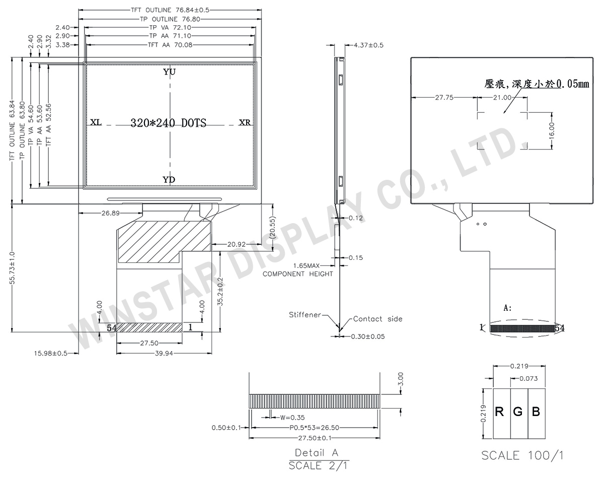
| Pin |
기호 |
기능 |
| 1~2 |
LED- |
Power for LED backlight cathode |
| 3~4 |
LED+ |
Power for LED backlight anode |
| 5 |
YU |
Top electrode |
| 6 |
XL |
Left electrode |
| 7 |
NC |
No connect |
| 8 |
/RESET |
Hardware reset |
| 9 |
SPENA |
Chip select pin of serial interface |
| 10 |
SPCLK |
Clock pin of serial interface |
| 11 |
SPDAT |
Data input pin in serial mode |
| 12~19 |
B0~B7 |
Data bus |
| 20~27 |
G0~G7 |
Data bus |
| 28~35 |
R0~R7 |
Data bus |
| 36 |
HSYNC |
Line synchronization signal |
| 37 |
VSYNC |
Frame synchronization signal |
| 38 |
DCLK |
Dot-clock signal and oscillator source |
| 39~40 |
NC |
No connect |
| 41~42 |
VCC |
Power Supply |
| 43 |
YD |
Bottom electrode |
| 44 |
XR |
Right electrode |
| 45~47 |
NC |
No connect |
| 48~50 |
SEL2~SEL0 |
Input pin to select input interface mode |
| 51 |
NC |
No connect |
| 52 |
DE |
Display enable pin from controller. Internal pull high
Connect to VCCIO or floating if not used |
| 53 |
DGND |
System ground pin of the IC. Connect to system ground. |
| 54 |
AVSS |
Grounding for analog circuit. Connect to system ground |