 - WF70A7SZAHLNN0")
우리는 귀하의 프라이버시를 소중히 여깁니다
"모든 쿠키 허용"을 클릭하면 사이트 탐색을 개선하고, 사이트 사용을 분석하며, 마케팅 및 성능 노력에 도움을 주기 위해 쿠키를 귀하의 장치에 저장하는 데 동의한 것으로 간주됩니다. 이 주제에 대한 추가 정보는 당사의 정책에서 확인할 수 있습니다. 개인정보 보호정책


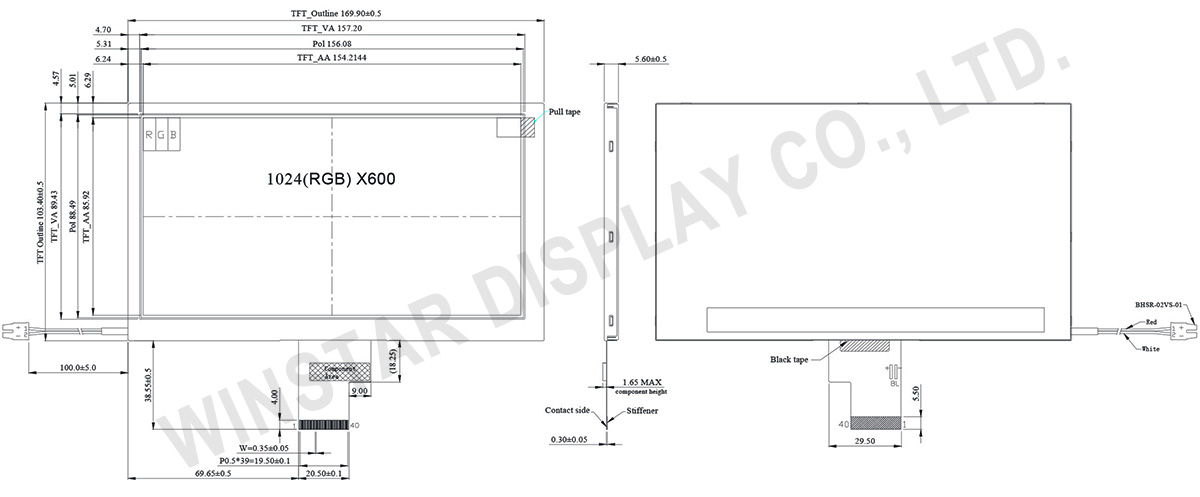
WF70A7SIAHLNN0은 1024x600 해상도를 가진 7인치 고휘도 TFT LCD 디스플레이 모듈로, 높은 가시성이 요구되는 응용 프로그램을 위해 설계되었습니다. 이 모듈은 1100 cd/m²의 밝기를 제공하여 대부분의 강한 빛 환경에서도 선명한 표시를 보장하며, 800:1의 높은 명암비로 생생한 색상과 풍부한 세부 사항을 제공합니다.
LVDS 인터페이스를 지원하여 안정적이고 효율적인 데이터 전송을 보장하며, 장시간 운영 및 고해상도 표시가 요구되는 응용 프로그램에 적합합니다. TFT 드라이버 IC(EK79001HE + EK73215BCGA)는 우수한 표시 성능을 제공하며, LED 백라이트는 최대 50,000시간의 수명을 가지며, -20°C에서 +70°C까지의 넓은 작동 온도 범위에서 안정적인 작동을 보장합니다.
모듈의 외형 크기는 169.90 x 103.40 mm이며, 활성 영역(AA 크기)은 154.2114 x 85.92 mm입니다. 이를 통해 야외 측정 장비, 산업 제어 시스템, 교통 모니터링, 정보 표시 등 다양한 응용 분야에 적합합니다. 다양한 환경 요구 사항을 충족할 수 있습니다. 또한, 모든 재료는 RoHS 및 REACH 환경 기준을 준수합니다.
| 항목 | 치수 | 단위 |
|---|---|---|
| 크기 | 7.0 | 인치 |
| 도트 매트릭스 | 1024 × RGB × 600(TFT) | 점 |
| 모듈 치수 | 169.9(W) × 103.4(H) × 5.6(D) | mm |
| 활성 영역 | 154.2114 × 85.92 | mm |
| 도트 피치 | 0.1506 × 0.1432 | mm |
| LCD 유형 | TFT, 백색, 투과성 | |
| 뷰 방향 | 12 o'clock | |
| 그레이스케일 반전 방향 | 6 o'clock | |
| 종횡비 | 16:9 | |
| 제어 IC | -- | |
| 드라이버 IC | EK79001HE + EK73215BCGA | |
| 역광 타입 | LED, 백색 | |
| 터치 패널 포함/제외 | 터치패널(스크린)이 없는 | |
| 인터페이스 | LVDS | |
| 표면 | 눈부심 방지 | |
| 항목 | 기호 | 최소값 | 대표값 | 최대값 | 단위 |
|---|---|---|---|---|---|
| 작동 온도 | TOP | -20 | - | +70 | ℃ |
| 보관 온도 | TST | -30 | - | +80 | ℃ |
| 항목 | 기호 | 표준값 | 단위 | ||
|---|---|---|---|---|---|
| 최소값 | 대표값 | 최대값 | |||
| Power voltage | DVDD | 3.0 | 3.3 | 3.6 | V |
| AVDD | 9.4 | 9.6 | 9.8 | V | |
| VGH | 17 | 18 | 19 | V | |
| VGL | -6.6 | -6.0 | -5.4 | V | |
| Input signal voltage | VCOM | 3.1 | 3.3 | 3.6 | V |
| Input logic high voltage | VIH | 0.7 DVDD | - | DVDD | V |
| Input logic low voltage | VIL | 0 | - | 0.3 DVDD | V |
| 항목 | 기호 | 표준값 | 단위 | ||
|---|---|---|---|---|---|
| 최소값 | 대표값 | 최대값 | |||
| Current for Driver | IGH | - | 0.2 | 1.0 | mA |
| IGL | - | 0.2 | 1.0 | mA | |
| IDVDD | - | 4.0 | 10 | mA | |
| IAVDD | - | 20 | 50 | mA | |
| 항목 | 기호 | 표준값 | 단위 | ||
|---|---|---|---|---|---|
| 최소값 | 대표값 | 최대값 | |||
| Voltage for LED backlight | VL | 16.8 | 19.2 | 21.0 | V |
| Current for LED backlight | IL | -- | 320 | -- | mA |
| LED life time | - | - | 50,000 | - | Hr |
| Pin No. | 기호 | I/O | 기능 |
|---|---|---|---|
| 1 | VCOM | P | Common Voltage |
| 2 | VDD | P | Digital circuit |
| 3 | VDD | P | Digital circuit |
| 4 | NC | --- | No connection |
| 5 | Reset | I | Global reset pin |
| 6 | STBYB | I | Standby mode, Normally pulled high STBYB = “1”, normal operation STBYB = “0”, timing controller, source driver will turn off, all output are High-Z |
| 7 | GND | P | Ground |
| 8 | RXIN0- | I | Negative LVDS differential data input |
| 9 | RXIN0+ | I | Positive LVDS differential data input |
| 10 | GND | P | Ground |
| 11 | RXIN1- | I | Negative LVDS differential data input |
| 12 | RXIN1+ | I | Positive LVDS differential data input |
| 13 | GND | P | Ground |
| 14 | RXIN2- | I | Negative LVDS differential data input |
| 15 | RXIN2+ | I | Positive LVDS differential data input |
| 16 | GND | P | Ground |
| 17 | RXCLKIN- | I | Negative LVDS differential clock input |
| 18 | RXCLKIN+ | I | Positive LVDS differential clock input |
| 19 | GND | P | Ground |
| 20 | RXIN3- | I | Negative LVDS differential data input |
| 21 | RXIN3+ | I | Positive LVDS differential data input |
| 22 | GND | P | Ground |
| 23 | NC | --- | No connection |
| 24 | NC | --- | No connection |
| 25 | GND | P | Ground |
| 26 | NC | --- | No connection |
| 27 | DIMO | O | Backlight CABC controller signal output |
| 28 | SELB | I | 6bit/8bit mode select H:6bit / L:8bit |
| 29 | AVDD | P | Power for Analog Circuit |
| 30 | GND | P | Ground |
| 31 | NC | --- | No connection |
| 32 | NC | --- | No connection |
| 33 | L/R | I | Horizontal inversion |
| 34 | U/D | I | Vertical inversion |
| 35 | VGL | P | Negative power for TFT |
| 36 | GND | P | Ground |
| 37 | GND | P | Ground |
| 38 | VGH | P | Positive power for TFT |
| 39 | NC | --- | No connection |
| 40 | NC | --- | No connection |

"모든 쿠키 허용"을 클릭하면 사이트 탐색을 개선하고, 사이트 사용을 분석하며, 마케팅 및 성능 노력에 도움을 주기 위해 쿠키를 귀하의 장치에 저장하는 데 동의한 것으로 간주됩니다. 이 주제에 대한 추가 정보는 당사의 정책에서 확인할 수 있습니다. 개인정보 보호정책