
 - WF50DSYA3MNN0")

 - WEN025664A")

우리는 귀하의 프라이버시를 소중히 여깁니다
"모든 쿠키 허용"을 클릭하면 사이트 탐색을 개선하고, 사이트 사용을 분석하며, 마케팅 및 성능 노력에 도움을 주기 위해 쿠키를 귀하의 장치에 저장하는 데 동의한 것으로 간주됩니다. 이 주제에 대한 추가 정보는 당사의 정책에서 확인할 수 있습니다. 개인정보 보호정책

 -128x64 해상도 - WEO012864ANX")
 -128x64 해상도 - WEO012864ANX")
 -128x64 해상도 - WEO012864ANX")
 -128x64 해상도 - WEO012864ANX")
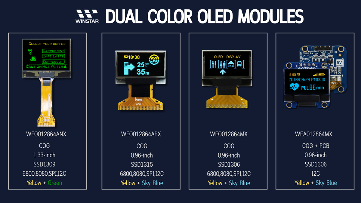
WEO012864ANX는 1.33인치 OLED 디스플레이 모듈로, 128x64 픽셀 해상도와 이색(노랑 + 초록) OLED 디스플레이를 제공합니다. 이 노란 OLED 및 초록 OLED 디스플레이는 높은 대비도와 낮은 전력 소모를 실현하여, 의료 기기, 산업 제어 시스템, 웨어러블 디바이스에 최적화되어 있습니다. SSD1309 IC 컨트롤러를 탑재하고 있으며, 6800, 8080, SPI, I2C 등 다양한 인터페이스 옵션을 지원하여 시스템 통합을 쉽게 할 수 있습니다.
Data source ref: WEO012864ANXAP3N00000
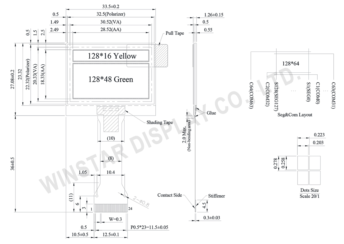
| 항목 | 치수 | 단위 |
|---|---|---|
| 도트 매트릭스 | 128 × 64 Dots | - |
| 모듈 치수 | 33.5 × 27.08 × 1.26 | mm |
| 활성 영역 | 28.52 × 18.33 | mm |
| 도트 크기 | 0.203 × 0.258 | mm |
| 도트 피치 | 0.223 × 0.278 | mm |
| 디스플레이 모드 | 패시브 매트릭스 (Passive Matrix) | |
| 디스플레이 색상 | 노란색과 초록색(이중 색상) | |
| Drive Duty | 1/64 Duty | |
| IC | SSD1309 | |
| 인터페이스 | 6800,8080,4-Wire SPI,I2C | |
| 크기 | 1.33 인치 | |
| 매개변수 | 기호 | 최소값 | 최대값 | 단위 |
|---|---|---|---|---|
| 논리용 전원 공급 전압 | VDD | -0.3 | 4 | V |
| 디스플레이 전원 공급 전압 | VCC | 0 | 17 | V |
| 작동 온도 | TOP | -40 | +80 | °C |
| 보관 온도 | TSTG | -40 | +85 | °C |
| 항목 | 기호 | 조건 | 최소값 | 대표값 | 최대값 | 단위 |
|---|---|---|---|---|---|---|
| 논리용 전원 공급 전압 | VDD | - | 1.65 | 3.0 | 3.5 | V |
| 디스플레이 전원 공급 전압 | VCC | - | 7.0 | 12.0 | 12.5 | V |
| 고전압 입력 | VIH | - | 0.8×VDD | - | - | V |
| 저전압 입력 | VIL | - | - | - | 0.2×VDD | V |
| 고전압 출력 | VOH | - | 0.9×VDD | - | - | V |
| 저전압 출력 | VOL | - | - | - | 0.1×VDD | V |
| 디스플레이 50% 픽셀 켜짐 | ICC | VCC=12V | - | 8.0 | 12.0 | mA |
| No. | 기호 | 기능 | |||||||||||||||
|---|---|---|---|---|---|---|---|---|---|---|---|---|---|---|---|---|---|
| 1 | ESD_GND | It should be connected to ground. | |||||||||||||||
| 2 | VLSS | This is an analog ground pin | |||||||||||||||
| 3 | VSS | Ground. | |||||||||||||||
| 4 | NC | No connection | |||||||||||||||
| 5 | VDD | Power supply pin for core logic operation | |||||||||||||||
| 6 | BS1 | MCU bus interface selection pins. Select appropriate logic setting as described in the following table. BS2 and BS1 are pin select
(1) 0 is connected to VSS (2) 1 is connected to VDD |
|||||||||||||||
| 7 | BS2 | ||||||||||||||||
| 8 | CS# | This pin is the chip select input connecting to the MCU. The chip is enabled for MCU communication only when CS# is pulled LOW (active LOW). |
|||||||||||||||
| 9 | RES# | This pin is reset signal input. When the pin is pulled LOW, initialization of the chip is executed. Keep this pin pull HIGH during normal operation. |
|||||||||||||||
| 10 | D/C# | This pin is Data/Command control pin connecting to the MCU. When the pin is pulled HIGH, the data at D[7:0] will be interpreted as data. When the pin is pulled LOW, the data at D[7:0] will be transferred to a command register. In I2C mode, this pin acts as SA0 for slave address selection. |
|||||||||||||||
| 11 | R/W# | This pin is read / write control input pin connecting to the MCU interface. When 6800 interface mode is selected, this pin will be used as Read/Write (R/W#) selection input. Read mode will be carried out when this pin is pulled HIGH and write mode when LOW. When 8080 interface mode is selected, this pin will be the Write (WR#) input. Data write operation is initiated when this pin is pulled LOW and the chip is selected. When serial or I2C interface is selected, this pin must be connected to VSS. |
|||||||||||||||
| 12 | E/RD# | This pin is MCU interface input. When 6800 interface mode is selected, this pin will be used as the Enable (E) signal. Read/write operation is initiated when this pin is pulled HIGH and the chip is selected. When 8080 interface mode is selected, this pin receives the Read (RD#) signal. Read operation is initiated when this pin is pulled LOW and the chip is selected. When serial or I2C interface is selected, this pin must be connected to VSS. |
|||||||||||||||
| 13-20 | D0~D7 | These pins are bi-directional data bus connecting to the MCU data bus. Unused pins are recommended to tie LOW. When serial interface mode is selected, D0 will be the serial clock input: SCLK; D1 will be the serial data input: SDIN and D2 should be kept NC. When I2C mode is selected, D2, D1 should be tied together and serve as SDAout, SDAin in application and D0 is the serial clock input, SCL. |
|||||||||||||||
| 21 | IREF | This pin is the segment output current reference pin. IREF is supplied externally. |
|||||||||||||||
| 22 | VCOMH | COM signal deselected voltage level. A capacitor should be connected between this pin and VSS. |
|||||||||||||||
| 23 | VCC | Power supply for panel driving voltage. This is also the most positive power voltage supply pin. | |||||||||||||||
| 24 | ESD_GND | It should be connected to ground. |

"모든 쿠키 허용"을 클릭하면 사이트 탐색을 개선하고, 사이트 사용을 분석하며, 마케팅 및 성능 노력에 도움을 주기 위해 쿠키를 귀하의 장치에 저장하는 데 동의한 것으로 간주됩니다. 이 주제에 대한 추가 정보는 당사의 정책에서 확인할 수 있습니다. 개인정보 보호정책