우리는 귀하의 프라이버시를 소중히 여깁니다
"모든 쿠키 허용"을 클릭하면 사이트 탐색을 개선하고, 사이트 사용을 분석하며, 마케팅 및 성능 노력에 도움을 주기 위해 쿠키를 귀하의 장치에 저장하는 데 동의한 것으로 간주됩니다. 이 주제에 대한 추가 정보는 당사의 정책에서 확인할 수 있습니다. 개인정보 보호정책


| Pin No. | 기호 | Level | 설명 | |||||||||||||||
|---|---|---|---|---|---|---|---|---|---|---|---|---|---|---|---|---|---|---|
| 1 | IRS | I | This terminal selects the resistors for the V0 voltage level adjustment. IRS = “H”: Use the internal resistors IRS = “L”: Do not use the internal resistors. The V0 voltage level is regulated by an external resistive voltage divider attached to the VR terminal |
|||||||||||||||
| 2 | /HPM | I | This is the power control terminal for the power supply circuit for liquid crystal drive. /HPM = “H”: Normal mode /HPM = “L”: High power mode (Default) |
|||||||||||||||
| 3 | P/S | I | This is the parallel data input/serial data input switch terminal. P/S = “H”: Parallel data input. P/S = “L”: Serial data input. The following applies depending on the P/S status:
/RD (E) and /WR (R/W) are fixed to either “H” or “L”. With serial data input, It is impossible read data from RAM |
|||||||||||||||
| 4 | C86 | I | This is the MPU interface selection pin. C86 = “H”: 6800 Series MPU interface. C86 = “L”: 8080 Series MPU interface |
|||||||||||||||
| 5 | VR | I | Output voltage regulator terminal. Provides the voltage between VSS and V0 through a resistive voltage divider. IRS = “L” : the V0 voltage regulator internal resistors are not used. IRS = “H” : the V0 voltage regulator internal resistors are used. |
|||||||||||||||
| 6~10 | V0~V4 | Power supply | This is a multi-level power supply for the liquid crystal drive. | |||||||||||||||
| 11 | VRS | Power supply | This is the internal-output VREG power supply for the LCD power supply voltage regulator | |||||||||||||||
| 12 | CAP4+ | O | DC/DC voltage converter. | |||||||||||||||
| 13 | CAP2- | O | DC/DC voltage converter. Connect a capacitor between this terminal and the CAP2P terminal. | |||||||||||||||
| 14 | CAP2+ | O | DC/DC voltage converter. Connect a capacitor between this terminal and the CAP2N terminal. | |||||||||||||||
| 15 | CAP1+ | O | DC/DC voltage converter. Connect a capacitor between this terminal and the CAP1N terminal. | |||||||||||||||
| 16 | CAP1- | O | DC/DC voltage converter. Connect a capacitor between this terminal and the CAP1P terminal. | |||||||||||||||
| 17 | CAP3+ | O | DC/DC voltage converter. Connect a capacitor between this terminal and the CAP1N terminal. | |||||||||||||||
| 18 | CAP5+ | O | DC/DC voltage converter. | |||||||||||||||
| 19 | VOUT | O | DC/DC voltage converter. Connect a capacitor between this terminal and vss or VDD | |||||||||||||||
| 20 | VSS | Power supply | Ground | |||||||||||||||
| 21 | VDD | Power supply | Power supply | |||||||||||||||
| 22~29 | D7~D0 | I/O | Data bus line | |||||||||||||||
| 30 | /RD(E) | I | • When connected to 8080 series MPU, this pin is treated as the “/RD” signal of the 8080 MPU and is LOW-active. The data bus is in an output status when this signal is “L”. • When connected to 6800 series MPU, this pin is treated as the “E” signal of the 6800 MPU and is HIGH-active. This is the enable clock input terminal of the 6800 Series MPU. |
|||||||||||||||
| 31 | /WR(R/W) | I |
• When connected to 8080 series MPU, this pin is treated as the “/WR” signal of the 8080 MPU and is LOW-active. |
|||||||||||||||
| 32 | A0 | I | This is connect to the least significant bit of the normal MPU address bus, and it determines whether the data bits are data or command. A0 = “H”: Indicates that D0 to D7 are display data. A0 = “L”: Indicates that D0 to D7 are control data. |
|||||||||||||||
| 33 | /RES | I | When RES is set to “L”, the setting are initialized. | |||||||||||||||
| 34 | /CS1 | I | This is the chip select signal. |
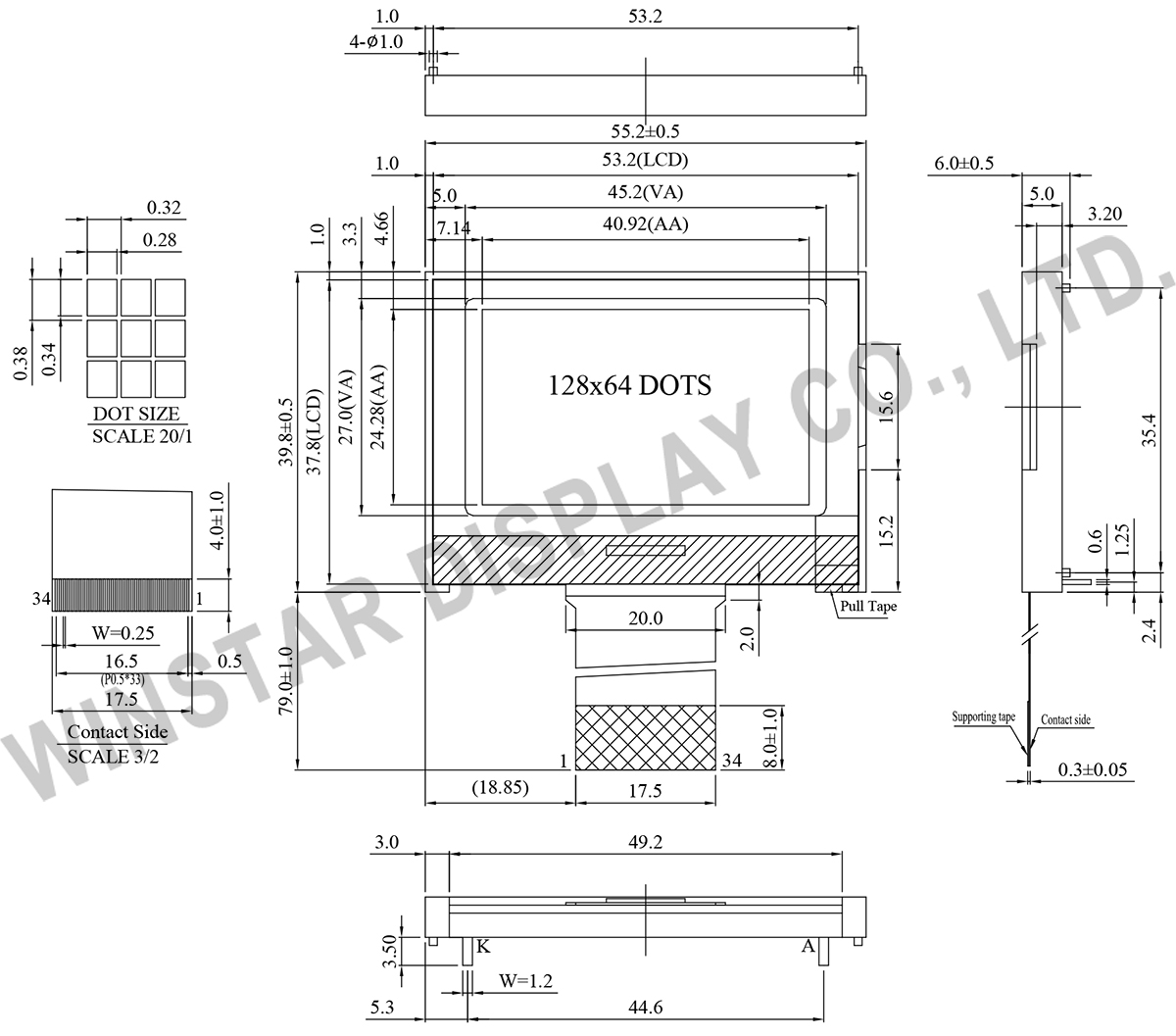
| 항목 | 치수 | 단위 |
|---|---|---|
| 점의 수 | 128 x 64 | - |
| 모듈 치수 | 55.2 x 39.8 x 6.5 | mm |
| 보기 영역 | 45.2 x 27.0 | mm |
| 활성 영역 | 40.92 x 24.28 | mm |
| 도트 크기 | 0.28 x 0.34 | mm |
| 도트 피치 | 0.32 x 0.38 | mm |
| 듀티 | 1/65 , 1/9 Bias | |
| 역광 타입 | LED | |
| IC | ST7565P | |
| 인터페이스 | 6800/8080/4-Line SPI | |
| 항목 | 기호 | 최소값 | 대표값 | 최대값 | 단위 |
|---|---|---|---|---|---|
| 작동 온도 | TOP | -20 | - | +70 | ℃ |
| 보관 온도 | TST | -30 | - | +80 | ℃ |
| Power Supply Voltage | VDD | -0.3 | - | 3.6 | V |
| Power supply voltage (VDD standard) | V0,VOUT | -0.3 | - | 14.5 | V |
| Power supply voltage (VDD standard) | V1,V2,V3,V4 | -0.3 | - | V0+0.3 | V |
| 항목 | 기호 | 조건 | 최소값 | 대표값 | 최대값 | 단위 |
|---|---|---|---|---|---|---|
| Supply Voltage For Logic | VDD-VSS | - | 2.7 | 3.0 | 3.3 | V |
| Supply Voltage For LCM | V0-VSS | Ta=-20℃ Ta=25℃ Ta=70℃ |
- 9.4 - |
- 9.6 - |
- 9.8 - |
V V V |
| Input High Volt. | VIH | - | 0.8 VDD | - | VDD | V |
| Input Low Volt. | VIL | - | VSS | - | 0.2VDD | V |
| Output High Volt. | VOH | - | 0.8VDD | - | VDD | V |
| Output Low Volt. | VOL | - | VSS | - | 0.2VDD | V |
| Supply Current(No include LED Backlight) | IDD | VDD=3.0V | - | 0.49 | 1.0 | mA |

"모든 쿠키 허용"을 클릭하면 사이트 탐색을 개선하고, 사이트 사용을 분석하며, 마케팅 및 성능 노력에 도움을 주기 위해 쿠키를 귀하의 장치에 저장하는 데 동의한 것으로 간주됩니다. 이 주제에 대한 추가 정보는 당사의 정책에서 확인할 수 있습니다. 개인정보 보호정책