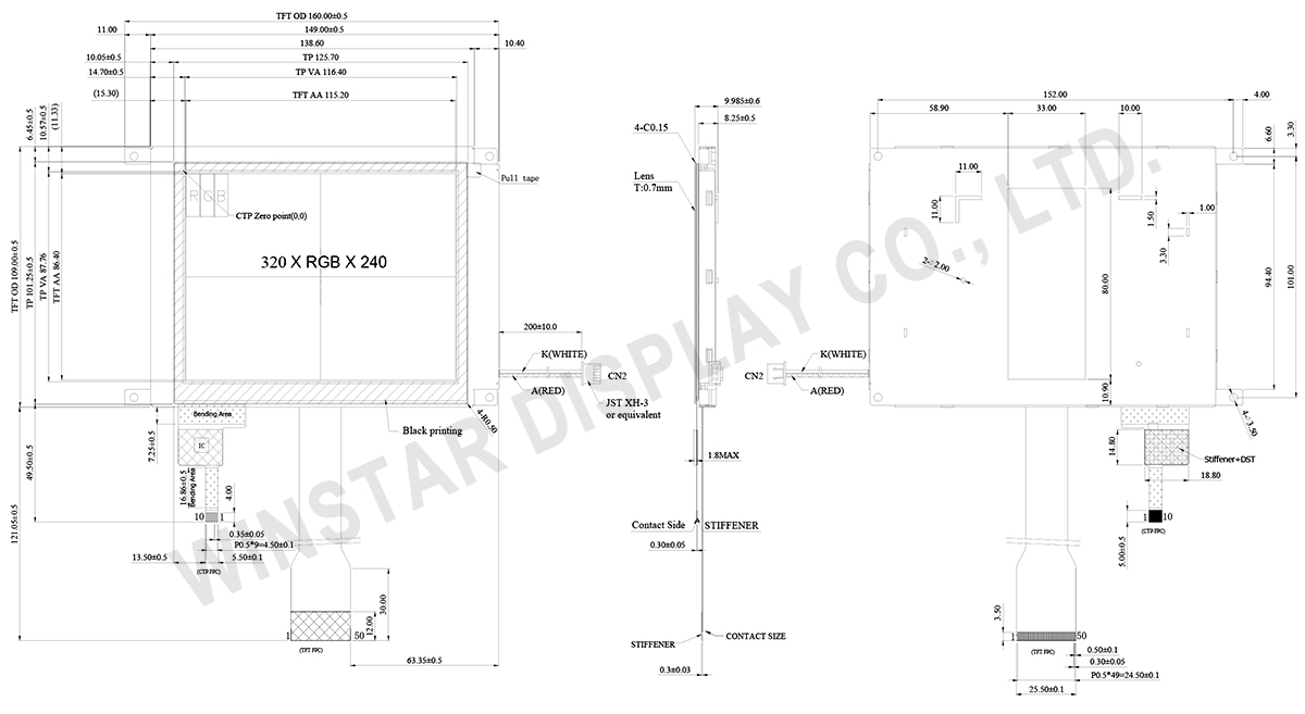
Home Prodotti Schermo TFT Display TFT Standard WF57VTIACDNG0

TFT 5.7" con Touch Screen Capacitivo

Modello numero WF57VTIACDNG0

►Dimensione : 5.7 pollici
►Risoluzione : 320 x 240 punti
►Direzione di visione : 12H
►Interfaccia : RGB
►Driver IC:HX8218+HX8615
►Scheda di controllo: No
►Luminosità (cd/m²) : 400
►Cornice di fissaggio : Yes
►Touch Screen : con pannello touch capacitivo (PCAP)
►Detect Point : 5 Fingers
►O-Film : Opzione

DISEGNO

5.7 inch Display, TFT LCD Touch Display - WF57VTIACDNG0

SPECIFICHE TECNICHE

Funzione dei Pin di Interfaccia

LCM PIN Definition

Pin Simbolo Funzione
1 IF1 Input data format control
2 IF2 Input data format control
3 POL Polarity Signal connect to VCOM driving circuit.
4 RESET Hardware reset
5 SPENA Chip select
6 SPCL Serial Clock
7 SPDA Serial Data
8 B0 Blue Data bit
9 B1 Blue Data bit
10 B2 Blue Data bit
11 B3 Blue Data bit
12 B4 Blue Data bit
13 B5 Blue Data bit
14 B6 Blue Data bit
15 B7 Blue Data bit
16 G0 Green Data bit
17 G1 Green Data bit
18 G2 Green Data bit
19 G3 Green Data bit
20 G4 Green Data bit
21 G5 Green Data bit
22 G6 Green Data bit
23 G7 Green Data bit
24 R0 Red Data bit
25 R1 Red Data bit
26 R2 Red Data bit
27 R3 Red Data bit
28 R4 Red Data bit
29 R5 Red Data bit
30 R6 Red Data bit
31 R7 Red Data bit
32 Hsync Horizontal synchronous signal
33 Vsync Vertical synchronous signal
34 Data CLK Dot data clock
35 AVDD(analog) Analog power: 4.5V~5.5V
36 AVDD(analog) Analog power: 4.5V~5.5V
37 VCC(Digital) Digital power: 3V~3.6V
38 VCC(Digital) Digital power: 3V~3.6V
39 NPC NTSC/PAL mode Auto detection result H:NTSC/L:PAL
40 VGL Gate off power
41 VGL Gate off power
42 UD Up/down selection
43 VGH Gate on power
44 LRC Shift direction of device internal shift register control.
45 GND System ground pin of the IC.
Connect to system ground.
46 VCOM VCOM driving input
47 VCOM VCOM driving input
48 ENB Signal to settle the horizontal display position
49 GND System ground pin of the IC.
Connect to system ground.
50 GND System ground pin of the IC.
Connect to system ground.

PCAP PIN Definition

Pin Simbolo Funzione
1 VSS System ground pin of the IC. Connect to system ground.
2 VDDT Power Supply : +3.0V
3 SCL I2C clock input
4 NC No connect
5 SDA I2C data input and output
6 NC No connect
7 /RST External Reset, Low is active
8 NC No connect
9 /INT External interrupt to the host
10 VSS System ground pin of the IC. Connect to system ground.

Specifiche generali

Articolo Dimensioni Unità
Dimensione 5.7 pollici
A matrice di punti 320 × RGB × 240 (TFT) dots
Dimensione del modulo 160(W) × 109(H) × 9.985 (D) mm
Area attiva 115.2 × 86.40 mm
Passo del Dot 0.12 × 0.36 mm
Tipo LCD TFT, Bianco, Trasmissivo
Direzione di visione 12 o'clock
Direzione di inversione della scala dei grigi 6 o'clock
TFT Interfaccia 24-bit RGB
TFT Drive IC HX8218+HX8615 o equivalente
Proporzioni dell’area visiva (ratio) 4:3
Tipo di backlight LED, Bianco
PCAP FW Version 0x07.0x00.0x00.0x00.0xA2.0x01.0x57.0x00
PCAP IC ILI2130 o equivalente
PCAP Interfaccia I2C
PCAP Risoluzione 16384*16384
Con / senza Touch Panel con pannello touch capacitivo(PCAP)
Superficie Bagliore (Glare)

Valori massimi assoluti

Articolo Simbolo Valore Min Valore tipico Valore massimo Unità
Temperatura di lavoro TOP -20 +70
Temperatura di stock TST -30 +80

Caratteristiche elettriche

Articolo Simbolo Valore Min Valore tipico Valore massimo Unità
Supply Voltage For LCM VCC 3.2 3.3 3.4 V
Supply Current For LCM ICC 30 45 mA
Supply PCAP VDDT 3.1 3.3 3.5 V
ICTP 56 84 mA
Input High Volt. VIH 0.7 VCC VCC V
Input Low Volt. VIL 0 0.3 VCC V
LCD Driving
Supply Voltage
VGH 15 16 17 V
VGL -6 -5 -4 V
VCOMH 4.5 V
VCOML -0.5 V
AVDD 4.5 5.0 5.5 V
go top
close