WF101JTYAHLNN0 è un modulo TFT LCD LVDS da 10.1 pollici con risoluzione 1024×600 e pannello IPS. Questo display LVDS è equipaggiato con driver IC EK79001HN ed EK73215BCGA e supporta un'interfaccia LVDS per una facile integrazione nei sistemi embedded.
Il display TFT LVDS offre ampi angoli di visione di 85/85/85/85 gradi e un rapporto di contrasto tipico di 800:1. Il modulo garantisce una luminosità tipica di 500 cd/m² e supporta un formato 16:9.
La tensione di alimentazione varia da 3,0V a 3,6V, con valore tipico di 3,3V. Il modulo supporta una temperatura operativa da -20°C a +80°C e una temperatura di stoccaggio da -30°C a +80°C.
Questo pannello TFT LCD LVDS è disponibile in diverse configurazioni touch, tra cui WF101JTYAHLNT0 con pannello touch resistivo (RTP) e WF101JTYAHLNB0 con pannello touch capacitivo proiettato (PCAP).
Per applicazioni che richiedono una luminosità superiore, è disponibile anche WF101JSYAHLNN0 come versione ad alta luminosità.
Il modulo LCD LVDS è adatto per apparecchiature di controllo industriale, dispositivi medicali, distributori automatici e sistemi embedded che richiedono un'integrazione stabile di display TFT.
SPECIFICHE TECNICHE
Specifiche generali
| Articolo |
Dimensioni |
Unità |
| Dimensione |
10.1 |
pollici |
| A matrice di punti |
1024 RGB x 600 |
dots |
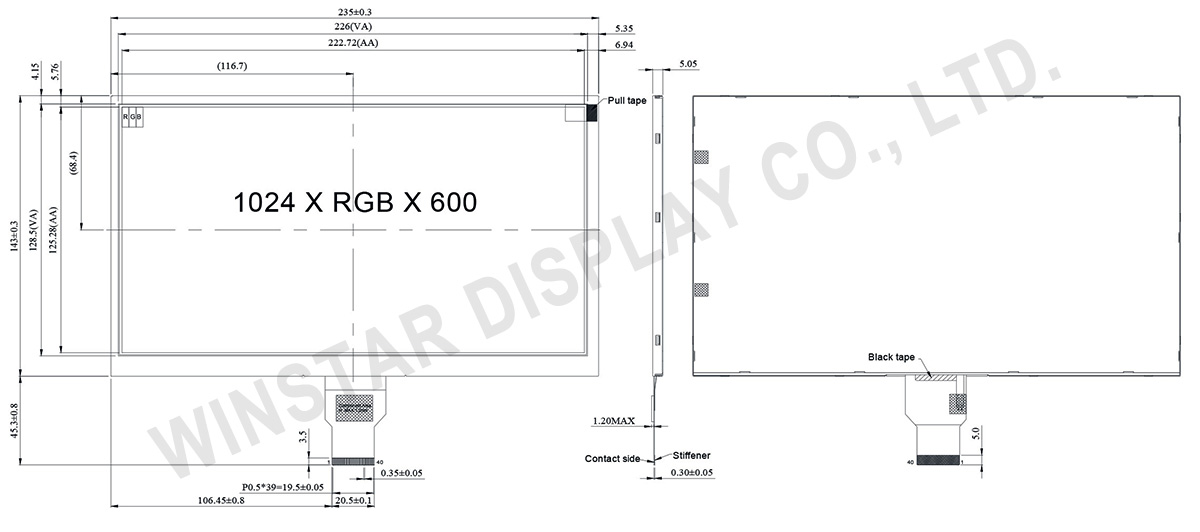
| Dimensione del modulo |
235(W) x 143(H) x 5.05(D) |
mm |
| Area attiva |
222.72 (H) x 125.28(V) |
mm |
| Passo del Dot |
0.2175(W) x 0.2088(H) |
mm |
| Tipo LCD |
TFT, Nero, Trasmissivo |
| Interfaccia |
LVDS |
| Driver IC |
EK79001HN + EK73215BCGA o equivalente |
| Direzione di visione |
85/85/85/85 |
| Proporzioni dell’area visiva (ratio) |
16:9 |
| Backlight Type |
LED, Bianco |
| Con / senza Touch Panel |
senza pannello touch (schermo) |
| Superficie |
Anti-Glare |
Valori massimi assoluti
| Articolo |
Simbolo |
Valore Min |
Valore tipico |
Valore massimo |
Unità |
| Temperatura di lavoro |
TOP |
-20 |
- |
+70 |
℃ |
| Temperatura di stock |
TST |
-30 |
- |
+80 |
℃ |
Caratteristiche elettriche
Typical Operation Conditions (At Ta = 25 °C,)
| Articolo |
Symbol |
Valore Min |
Valore tipico |
Valore massimo |
Unità |
| Digital Power Supply Voltage For LCD |
VDD |
3 |
3.3 |
3.6 |
V |
| Analog Power Supply Voltage |
AVDD |
9.89 |
10.2 |
10.5 |
V |
| Gate On Power Supply Voltage |
VGH |
19.4 |
20.0 |
20.6 |
V |
| Gate Off Power Supply Voltage |
VGL |
-10.3 |
-10.0 |
-9.7 |
V |
| Common Power Supply Voltage |
VCOM |
4.0 |
4.3 |
4.6 |
V |
| Input logic high voltage |
VIH |
0.7 VDD |
- |
VDD |
V |
| Input logic low voltage |
VIL |
0 |
- |
0.3 VDD |
V |
Funzione dei Pin di Interfaccia
| Pin No. |
Simbolo |
Funzione |
| 1 |
VCOM |
Common voltage |
| 2 |
VDD |
Digital power |
| 3 |
VDD |
Digital power |
| 4 |
NC |
Not connect |
| 5 |
Reset |
Global reset pin. Active low to enter reset state. Suggest to connecting with an RC reset circuit for stability. Normally pull high. (R=10KΩ,C=1μF) |
| 6 |
STBYB |
Standby mode, normally pull high STBYB=”1”, normal operation STBYB=”0”,timing control, source driver will turn off, all output are high-Z |
| 7 |
GND |
Digital ground |
| 8 |
RXIN0- |
Negative LVDS differential data inputs |
| 9 |
RXIN0+ |
Positive LVDS differential data inputs |
| 10 |
GND |
Digital ground |
| 11 |
RXIN1- |
Negative LVDS differential data inputs |
| 12 |
RXIN1+ |
Positive LVDS differential data inputs |
| 13 |
GND |
Digital ground |
| 14 |
RXIN2- |
Negative LVDS differential data inputs |
| 15 |
RXIN2+ |
Positive LVDS differential data inputs |
| 16 |
GND |
Digital ground |
| 17 |
RXCLKN- |
Negative LVDS differential clock inputs |
| 18 |
RXCLKN+ |
Positive LVDS differential clock inputs |
| 19 |
GND |
Digital ground |
| 20 |
RXIN3- |
Negative LVDS differential data inputs |
| 21 |
RXIN3+ |
Positive LVDS differential data inputs |
| 22 |
GND |
Digital ground |
| 23 |
NC |
Not connect |
| 24 |
NC |
Not connect |
| 25 |
GND |
Digital ground |
| 26 |
NC |
Not connect |
| 27 |
NC |
Not connect |
| 28 |
SELB |
6-bit/8-bit input select SELB = L , 8-bit ; SELB = H , 6-bit |
| 29 |
AVDD |
Analog power |
| 30 |
GND |
Digital ground |
| 31 |
LED- |
LED Cathode |
| 32 |
LED- |
LED Cathode |
| 33 |
L/R |
Left or right display control |
| 34 |
U/D |
Up / down display control |
| 35 |
VGL |
Negative power for TFT |
| 36 |
NC |
Not connect |
| 37 |
NC |
Not connect |
| 38 |
VGH |
Positive power for TFT |
| 39 |
LED+ |
LED Anode |
| 40 |
LED+ |
LED Anode |
When L/R=”0”,set right to left scan direction.
When L/R=”1”,set left to right scan direction.
When U/D=”0”,set top to bottom scan direction.
When U/D=”1”,set bottom to top scan direction.