WF101JTYAHLNN0 es una pantalla TFT LCD LVDS de 10,1 pulgadas con resolución 1024×600 y panel IPS. Este modelo incorpora los controladores EK79001HN y EK73215BCGA y admite una interfaz LVDS para integración en sistemas embebidos.
La pantalla TFT LVDS ofrece amplios ángulos de visión de 85/85/85/85 grados y una relación de contraste típica de 800:1. El módulo proporciona un brillo típico de 500 cd/m² y formato de pantalla 16:9.
El módulo funciona con un rango de alimentación de 3,0V a 3,6V, con un valor típico de 3,3V. Admite un rango de temperatura de funcionamiento de -20°C a +80°C y un rango de almacenamiento de -30°C a +80°C.
Esta pantalla TFT LCD LVDS está disponible en diferentes configuraciones táctiles, incluyendo WF101JTYAHLNT0 con panel táctil resistivo (RTP) y WF101JTYAHLNB0 con panel táctil capacitivo proyectado (PCAP).
Para aplicaciones que requieren mayor brillo, también está disponible WF101JSYAHLNN0 como versión de alto brillo.
El módulo es adecuado para equipos de control industrial, dispositivos médicos, máquinas expendedoras y sistemas embebidos que requieren una integración fiable de pantalla TFT.
ESPECIFICACIONES
Especificaciones generales
| Elemento |
Dimensión |
Unidad |
| Tamaño |
10.1 |
pulgada |
| Matriz de puntos |
1024 RGB x 600 |
dots |
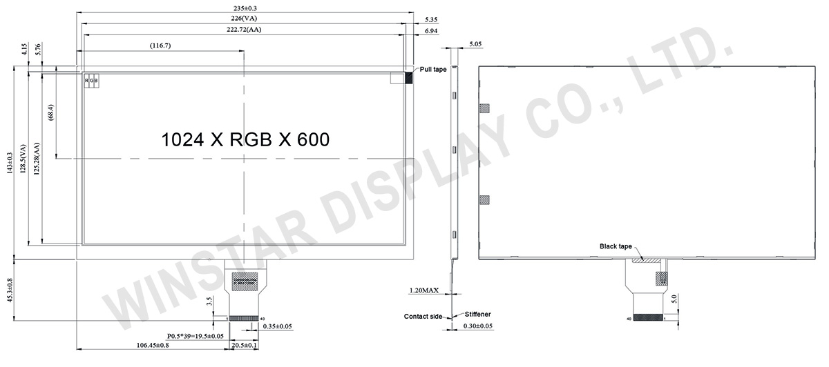
| Dimensión del módulo |
235(W) x 143(H) x 5.05(D) |
mm |
| zona activa |
222.72 (H) x 125.28(V) |
mm |
| Distancia entre puntos |
0.2175(W) x 0.2088(H) |
mm |
| Tipo de LCD |
TFT, Negro, Transmisivo |
| Interfaz |
LVDS |
| Controlador IC |
EK79001HN + EK73215BCGA o equivalente |
| Dirección de la vista |
85/85/85/85 |
| Relación de aspecto |
16:9 |
| Tipo de retroiluminación |
LED, Blanco |
| Con o sin panel táctil |
Sin panel táctil |
| Superficie |
Pantalla antirreflectante |
Valores nominales máximos absolutos
| Elemento |
Símbolo |
Valor mín. |
Valor típico |
Valor máx. |
Unidad |
| Temperatura de funcionamiento |
TOP |
-20 |
- |
70 |
℃ |
| Temperatura de almacenamiento |
TST |
-20 |
- |
70 |
℃ |
Características electrónicas
Typical Operation Conditions (At Ta = 25 °C,)
| Elemento |
Símbolo |
Valor mín. |
Valor típico |
Valor máx. |
Unidad |
| Digital Power Supply Voltage For LCD |
VDD |
3 |
3.3 |
3.6 |
V |
| Analog Power Supply Voltage |
AVDD |
9.89 |
10.2 |
10.5 |
V |
| Gate On Power Supply Voltage |
VGH |
19.4 |
20.0 |
20.6 |
V |
| Gate Off Power Supply Voltage |
VGL |
-10.3 |
-10.0 |
-9.7 |
V |
| Common Power Supply Voltage |
VCOM |
4.0 |
4.3 |
4.6 |
V |
| Input logic high voltage |
VIH |
0.7 VDD |
- |
VDD |
V |
| Input logic low voltage |
VIL |
0 |
- |
0.3 VDD |
V |
Función interfaz Pin
| Pin No. |
Símbolo |
Función |
| 1 |
VCOM |
Common voltage |
| 2 |
VDD |
Digital power |
| 3 |
VDD |
Digital power |
| 4 |
NC |
Not connect |
| 5 |
Reset |
Global reset pin. Active low to enter reset state. Suggest to connecting with an RC reset circuit for stability. Normally pull high. (R=10KΩ,C=1μF) |
| 6 |
STBYB |
Standby mode, normally pull high STBYB=”1”, normal operation STBYB=”0”,timing control, source driver will turn off, all output are high-Z |
| 7 |
GND |
Digital ground |
| 8 |
RXIN0- |
Negative LVDS differential data inputs |
| 9 |
RXIN0+ |
Positive LVDS differential data inputs |
| 10 |
GND |
Digital ground |
| 11 |
RXIN1- |
Negative LVDS differential data inputs |
| 12 |
RXIN1+ |
Positive LVDS differential data inputs |
| 13 |
GND |
Digital ground |
| 14 |
RXIN2- |
Negative LVDS differential data inputs |
| 15 |
RXIN2+ |
Positive LVDS differential data inputs |
| 16 |
GND |
Digital ground |
| 17 |
RXCLKN- |
Negative LVDS differential clock inputs |
| 18 |
RXCLKN+ |
Positive LVDS differential clock inputs |
| 19 |
GND |
Digital ground |
| 20 |
RXIN3- |
Negative LVDS differential data inputs |
| 21 |
RXIN3+ |
Positive LVDS differential data inputs |
| 22 |
GND |
Digital ground |
| 23 |
NC |
Not connect |
| 24 |
NC |
Not connect |
| 25 |
GND |
Digital ground |
| 26 |
NC |
Not connect |
| 27 |
NC |
Not connect |
| 28 |
SELB |
6-bit/8-bit input select SELB = L , 8-bit ; SELB = H , 6-bit |
| 29 |
AVDD |
Analog power |
| 30 |
GND |
Digital ground |
| 31 |
LED- |
LED Cathode |
| 32 |
LED- |
LED Cathode |
| 33 |
L/R |
Left or right display control |
| 34 |
U/D |
Up / down display control |
| 35 |
VGL |
Negative power for TFT |
| 36 |
NC |
Not connect |
| 37 |
NC |
Not connect |
| 38 |
VGH |
Positive power for TFT |
| 39 |
LED+ |
LED Anode |
| 40 |
LED+ |
LED Anode |
When L/R=”0”,set right to left scan direction.
When L/R=”1”,set left to right scan direction.
When U/D=”0”,set top to bottom scan direction.
When U/D=”1”,set bottom to top scan direction.