
 配備鐵框 - WEF012864U")
 配備鐵框 - WEF012864U")
 配備鐵框 - WEF012864U")
 配備鐵框 - WEF012864U")
 配備鐵框 - WEF012864U")
 配備鐵框 - WEF012864U")
 配備鐵框 - WEF012864U")
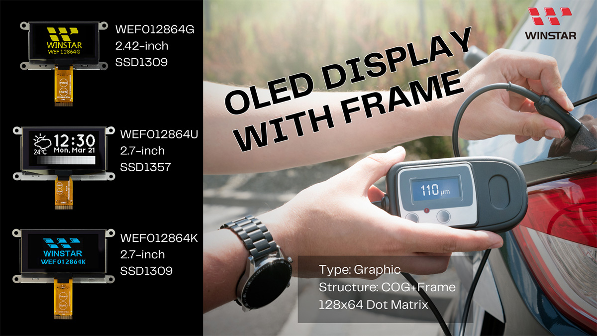
產品敘述
WEF012864U是一款COG圖形2.7吋單色被動式矩陣顯示模組(PMOLED)加鐵框,面板解析度為128x64像素且具高對比度(10,000:1)與4 bits支援灰階。 WEF012864U內建SSD1357控制器IC,支援多種傳輸介面:6800/8080 8-bit 並列介面,I2C與4線SPI介面,採用3V驅動。
相同的 OLED 面板還可參考:
- WEO012864U 系列採用無鐵框設計。
- WEP012864U 系列採用鐵框+PCB板,不用額外開發PCB板並整合介面設定和VCC電路,簡化使用者體驗。
- 除了鐵框和PCB板外,WEP012864U-CTP 系列還增加了 CTP 觸控功能。
WEF012864K是一款COG結構的OLED顯示模組。 它是有機自發光的,不需要背光。 此模組輕薄、功耗低。 WEF012864K模組非常適合手持產品、測量儀器、家用產品、POS系統、物聯網、通訊設備和醫療設備等。此模組的工作溫度為-40℃至+80℃,儲存溫度為-40℃至+80℃ 。為-40℃至+85℃。
規格圖
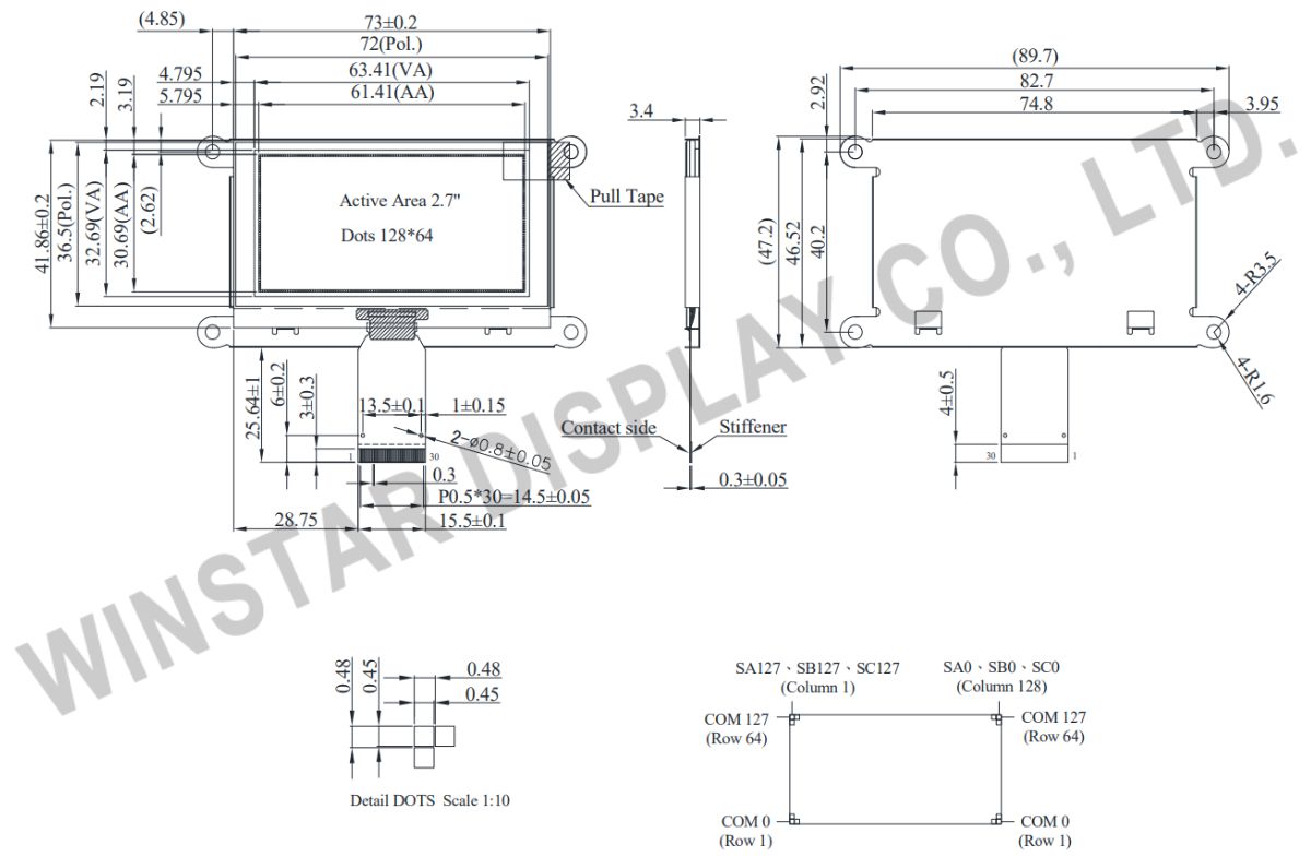
Data source ref:WEF012864ULPP3N00000
產品規格
Pin功能定義
| Pin No. | 符號 | 功能說明 | |||||||||||||||
|---|---|---|---|---|---|---|---|---|---|---|---|---|---|---|---|---|---|
| 1 | NC(GND) | No connection | |||||||||||||||
| 2 | VSS | Ground of Logic Circuit. This is a ground pin. It also acts as a reference for the logic pins. It must be connected to external ground. |
|||||||||||||||
| 3 | VCC | Power supply for panel driving voltage. This is also the most positive power voltage supply pin. | |||||||||||||||
| 4 | VCOMH | Voltage Output High Level for COM Signal. This pin is the input pin for the voltage output high level for COM signals. A tantalum capacitor should be connected between this pin and VSS. |
|||||||||||||||
| 5 | VLSS | Ground of Analog Circuit These are the analog ground pins. They should be connected to VSS externally. |
|||||||||||||||
| 6~13 | D7~D0 | These pins are bi-directional data bus connecting to the MCU data bus.Unused pins are recommended to tie LOW. When serial interface mode is selected, D0 will be the serial clock input: SCLK; D1 will be the serial data input: SDIN and D2 should be kept NC. When I2C mode is selected, D2, D1 should be tied together and serve as SDAout,SDAin in application and D0 is the serial clock input, SCL. |
|||||||||||||||
| 14 | E/RD# | This pin is MCU interface input. When 6800 interface mode is selected, this pin will be used as the Enable (E) signal. Read/write operation is initiated when this pin is pulled HIGH and the chip is selected. When 8080 interface mode is selected, this pin receives the Read (RD#) signal. Read operation is initiated when this pin is pulled LOW and the chip is selected. When serial or I2C interface is selected, this pin must be connected to VSS. |
|||||||||||||||
| 15 | R/W# | This pin is read / write control input pin connecting to the MCU interface. When 6800 interface mode is selected, this pin will be used as Read/Write (R/W#) selection input. Read mode will be carried out when this pin is pulled HIGH and write mode when LOW. When 8080 interface mode is selected, this pin will be the Write (WR#) input. Data write operation is initiated when this pin is pulled LOW and the chip is selected. When serial or I2C interface is selected, this pin must be connected to VSS. |
|||||||||||||||
| 16 17 |
BS1 BS2 |
Communicating Protocol Select. These pins are MCU interface selection input. See the following table:
|
|||||||||||||||
| 18 | D/C# | This pin is Data/Command control pin connecting to the MCU. When the pin is pulled HIGH, the data at D[7:0] will be interpreted as data. When the pin is pulled LOW, the data at D[7:0] will be transferred to a command register. In I2C mode, this pin acts as SA0 for slave address selection.When 3-wire serial interface is selected, this pin must be connected to VSS. |
|||||||||||||||
| 19 | CS# | Chip SelectThis pin is the chip select input. The chip is enabled for MCU communication onlywhen CS# is pulled low. |
|||||||||||||||
| 20 | RES# | This pin is reset signal input. When the pin is pulled LOW, initialization of the chip is executed.Keep this pin pull HIGH during normal operation. |
|||||||||||||||
| 21 | FR | Frame Frequency Triggering Signal This pin will send out a signal that could be used to identify the driver status. Nothing should be connected to this pin. It should be left open individually. |
|||||||||||||||
| 22 | IREF | This pin is the segment output current reference pin. IREF is supplied externally. |
|||||||||||||||
| 23 | N.C | Reserved Pin The N.C. pin between function pins is reserved for compatible and flexible design. |
|||||||||||||||
| 24 | VDD | Power Supply for I/O Pin. This pin is a power supply pin of I/O buffer. It should be connected to VCI or external source. All I/O signal should have VIH reference to VDDIO. When I/O signal pins (BS0~BS1, D0~D7, control signals…) pull high, they should be connected to VDDIO. |
|||||||||||||||
| 25 | VP | Power Supply for Core Logic Circuit This is a voltage supply pin. It can be supplied externally (within the range of 2.4~2.6V) or regulated internally from VCI. A capacitor should be connected between this pin & VSS under all circumstances. |
|||||||||||||||
| 26 | VDD | Power Supply for Operation. This is a voltage supply pin. It must be connected to external source & always be equal to or higher than VDD & VDDIO. |
|||||||||||||||
| 27 | VSL | Voltage Output Low Level for SEG Signal This is segment voltage (output low level) reference pin. This pin has to connect with resistor and diode to ground (details depends on application). |
|||||||||||||||
| 28 | VLSS | Ground of Analog Circuit These are the analog ground pins. They should be connected to VSS externally. |
|||||||||||||||
| 29 | VLSS | Power Supply for OEL Panel These are the most positive voltage supply pin of the chip. They must be connected to external source. |
|||||||||||||||
| 30 | NC(GND) | No connection |
規格說明
| 項目 | 規格 | 單位 |
|---|---|---|
| 點陣(解析度) | 128 × 64 | dots |
| 模組尺寸 | 89.7 × 47.2 ×3.4 | mm |
| 有效區域 | 64..41 × 30.69 | mm |
| 像素大小 | 0.45 × 0.45 | mm |
| 像素間距 | 0.48 × 0.48 | mm |
| 顯示模式 | 被動矩陣 | |
| 發光顏色 | 單色 | |
| 驅動方式 | 1/64 Duty | |
| 灰階 | 4 bits | |
| IC | SSD1357 | |
| 介面 | 8-bits 6800 and 8080 parallel, 4-line SPI, I2C | |
| 尺寸(對角線) | 2.7 吋 | |
最大絕對額定值
| 參數 | 符號 | 最小值 | 最大值 | 單位 |
|---|---|---|---|---|
| 邏輯電源電壓 | VDD | -0.3 | 4 | V |
| 顯示電源電壓 | VCC | 0 | 15 | V |
| 工作溫度 | TOP | -40 | +80 | °C |
| 儲存溫度 | TSTG | -40 | +85 | °C |
電氣特性
DC 電氣特性
| 項目 | 符號 | 條件 | 最小值 | 典型值 | 最大值 | 單位 |
|---|---|---|---|---|---|---|
| 邏輯電源電壓 | VDD | - | 1.65 | 3.0 | 3.3 | V |
| 顯示電源電壓 | VCC | - | 8.0 | 9.0 | 9.5 | V |
| 輸入高準位 | VIH | - | 0.8×VDD | - | VDD | V |
| 輸入低準位 | VIL | - | 0 | - | 0.2×VDD | V |
| 輸出高準位 | VOH | - | 0.9×VDD | - | VDD | V |
| 輸出低準位 | VOL | - | 0 | - | 0.1×VDD | V |
| Display 50% Pixel on | ICC | VCC =9V | - | 31.5 | 47.5 | mA |
Search keyword: 128x64 oled, oled 128x64, 2.7 oled, 2.7 吋 oled, oled 2.7
