


Олед дисплей 1.92", 160x128
Артикул. WEO160128B
►Тип: Графический
►Тип монтажа контроллера: COG
►Диагональ: 1.92 дюйма
►Разрешение: 160 x 128 точек
►IC:CH1120
►3V Power supply
►1/128 duty
►Интерфейс: 6800, 8080, SPI, I2C
►Цвет дисплея: Белый
►Инверсия
Описание
WEO160128B – это новый 1.92'' дюймовый COG OLED дисплей c разрешением 160x128 точек. Модуль сделан на базе контроллера IC CH1120 c поддержкой интерфейсов: параллельного 6800/8080 8-Бит, I2C и четырехжильного SPI интерфейса. Напряжение питания 3V, напряжение питания для логики дисплея 12V c рабочим циклом 1/128. Данный OLED дисплей обладает высоким контрастом - 10,000:1 (типичное значение) и 4-х битной градацией серого.
WEO0160128A может работать при температурах от -40 ° С до + 80 ℃, а температура хранения - от -40 ℃ до + 85 ℃. В настоящее время индикатор доступен в белом цвете; другие цвета находятся в стадии разработки и будут скоро доступны.
Данный индикатор идеально подходит для применения в носимых измерительных приборах, измерительных приборах промышленного применения, POS системах, Облачных/IoT системах, умных устройствах, автомобилестроении, коммуникационных системах, медицинских устройствах и т.д.
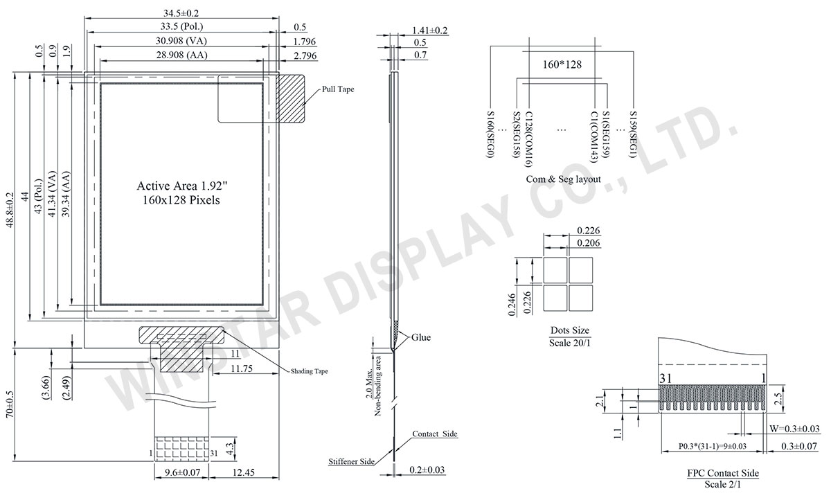
Чертеж
Data source ref: WEO160128BWPP3N00000
Технические характеристики
Функции контроллера контактного интерфейса
| No. | Символы | Описание | ||||||||||||||||||||||||
|---|---|---|---|---|---|---|---|---|---|---|---|---|---|---|---|---|---|---|---|---|---|---|---|---|---|---|
| 1 | NC | No connection | ||||||||||||||||||||||||
| 2 | VPP | This is the most positive voltage supply pad of the chip. It should be supplied externally. |
||||||||||||||||||||||||
| 3 | VSEGM | This is a segment pre-charge voltage. A capacitor can be connected between this pad and VSS if necessary. When external capacitor Is not used, this pin should be kept NC. |
||||||||||||||||||||||||
| 4 | VCOMH | This is a pad for the voltage output high level for common signals. A capacitor should be connected between this pad and VSS. |
||||||||||||||||||||||||
| 5 | VSL | Discharge voltage level pad. This pad should be connected to resistor and diode externally. |
||||||||||||||||||||||||
| 6 | NC | No connection | ||||||||||||||||||||||||
| 7 | IREF | This is a segment current reference pad. A resistor should be connected between this pad and VSS. . |
||||||||||||||||||||||||
| 8 | VPP | This is the most positive voltage supply pad of the chip. It should be supplied externally. |
||||||||||||||||||||||||
| 9 | NC | No connection | ||||||||||||||||||||||||
| 10 | VSS | Ground for logic and analog. This pad should be connected to GND externally. | ||||||||||||||||||||||||
| 11 | VCL | This is a common voltage reference pad. This pad should be connected to VSS externally. |
||||||||||||||||||||||||
| 12 | VDD | Power supply for logic and input/output | ||||||||||||||||||||||||
| 13 | IM0 | These are the MPU interface mode select pads.
|
||||||||||||||||||||||||
| 14 | IM1 | |||||||||||||||||||||||||
| 16 | IM2 | |||||||||||||||||||||||||
| 15 | VDD | Power supply for logic and input/output | ||||||||||||||||||||||||
| 17 | CS | This pad is the chip select input. When CSB = "L", then the chip select becomes active, and data command I/O is enabled. When in I2C interface, this pin is not used, so it must be connected to "L". | ||||||||||||||||||||||||
| 18 | RES | This is a reset signal input pad. When RESB is set to "L", the settings are initialized. The reset operation is performed by the RESB signal level. This pin internal pull high. | ||||||||||||||||||||||||
| 19 | A0 | This is the Data/Command control pad that determines whether the data bits are data or a command. A0 = "H ": the inputs at D0 to D7 are treated as display data. A0 = "L ": the inputs at D0 to D7 are transferred to the command registers. In I2C interface, this pad serves as SA0 to distinguish the different address of OLED driver. When in 3-wire interface, this pin is not used, so it must be connected to "L ". |
||||||||||||||||||||||||
| 20 | WR | This is a MPU interface input pad. When connected to an 8080 MPU, this is active LOW. This pad connects to the 8080 MPU WR signal. The signals on the data bus are latched at the rising edge of the WR signal. When connected to a 6800 Series MPU: This is the read/write control signal input terminal. When R/W = "H ": Read. When R/W = "L ": Write. When in 3-wire.4-wire & I2C interface, this pin is not used, so it must be connected to "L ". |
||||||||||||||||||||||||
| 21 | RD | This is a MPU interface input pad. When connected to an 8080 series MPU, it is active LOW. This pad is connected to the RD signal of the 8080 series MPU, and the data bus is in an output status when this signal is "L". When connected to a 6800 series MPU, this is active HIGH. This is used as an enable clock input of the 6800 series MPU. When in 3-wire.4-wire & I2C interface, this pin is not used, so it must be connected to "L". |
||||||||||||||||||||||||
| 22 | D0 | This is an 8-bit bi-directional data bus that connects to an 8-bit or 16-bit standard MPU data bus. When the serial interface(SPI) and I2C is selected, then D0 serves as the serial clock input pad (SCL) and D1 serves as the serial data input pad (SI). At this time, D2 to D7 are set to high impedance. D7~D2 is recommended to connect the VDD or GND. It is also allowed to leave D7~D2 unconnected. |
||||||||||||||||||||||||
| 23 | D1 | |||||||||||||||||||||||||
| 24 | D2 | |||||||||||||||||||||||||
| 25 | D3 | |||||||||||||||||||||||||
| 26 | D4 | |||||||||||||||||||||||||
| 27 | D5 | |||||||||||||||||||||||||
| 28 | D6 | |||||||||||||||||||||||||
| 29 | D7 | |||||||||||||||||||||||||
| 30 | NC | No connection | ||||||||||||||||||||||||
| 31 | VPP | This is the most positive voltage supply pad of the chip. It should be supplied externally. |
Механические характеристики
| Наименование | Измерения | Единица |
|---|---|---|
| Разрешение | 128 × 160 | точек |
| Габариты | 34.5 × 48.8 × 1.41 | mm |
| Активная область | 28.908 × 39.34 | mm |
| Размер пикселя | 0.206 × 0.226 | mm |
| Шаг пикселя | 0.226 × 0.246 | mm |
| Матрица | Пассивная | |
| Цвет дисплея | монохромные | |
| Рабочий цикл | 1/128 Duty | |
| IC | CH1120 | |
| Интерфейс | 6800, 8080, SPI, I2C | |
| Диагональ | 1.92 дюйма | |
Абсолютные максимальные значения
| Параметр | Символы | Минимальный | Максимальный | Единица |
|---|---|---|---|---|
| Supply Voltage for Logic | VDD | -0.3 | 3.5 | V |
| Supply Voltage for Display | VPP | -0.3 | 15.0 | V |
| Operating Temperature | TOP | -40 | +80 | °C |
| Storage Temperature | TSTG | -40 | +85 | °C |
Электронные характеристики
| Наименование | Символы | Кондиция | Минимальный | Типичный | Максимальный | Единица |
|---|---|---|---|---|---|---|
| Supply Voltage for Logic | VDD | - | 1.65 | 3.0 | 3.5 | V |
| Supply Voltage for Display | VPP | - | 11.5 | 12.0 | 12.5 | V |
| Input High Volt. | VIH | - | 0.8xVDD | - | VDD | V |
| Input Low Volt. | VIL | - | VSS | - | 0.2xVDD | V |
| Output High Volt. | VOH | IOH=-0.5mA | 0.8xVDD | - | VDD | V |
| Output Low Volt. | VOL | IOL=0.5mA | VSS | - | 0.2xVDD | V |
| Display 50% Pixel on | IPP | VPP=12V | - | 25 | 37.5 | mA |
