


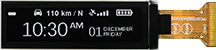
256×64 OLED 2.08 дюйма
Артикул. WEO025664A
►Тип: Графический
►Тип монтажа контроллера: COG
►Диагональ: 2.08 дюйма
►Разрешение: 256 x 64 точек
►IC:SSD1362
►3V Power supply
►1/64 duty
►Интерфейс: 6800, 8080, SPI, I2C
►Цвет дисплея: Белый / Желтый
►Инверсия
►Other FPC options available in below table
Описание
WEO025664A – 2.08" дюймовый Графический COG OLED модуль с разрешением 256x64 точки c шлейфом для пайки. Дисплей WEO025664A сделан на базе контроллера IC SSD1362 c поддержкой интерфейсов: параллельного 6800/8080 8-Бит, I2C и 3-х/4-х жильного SPI интерфейса. Напряжение питания 3V, 1/64 рабочий цикл.
Данный 2.08"-дюймовый ультратонкий (1.61 mm) и легкий OLED модуль идеально подходит для: приборов умного дома, измерительных приборов, приборов для личной гигиены, умных устройств, медицинских устройств и т.д. WEO025664A может работать при температурах от -40℃ до + 80℃; а температура хранения - от -40℃ до +85℃. Ниже приведена основная спецификация:
 FPC Options
 Чертеж
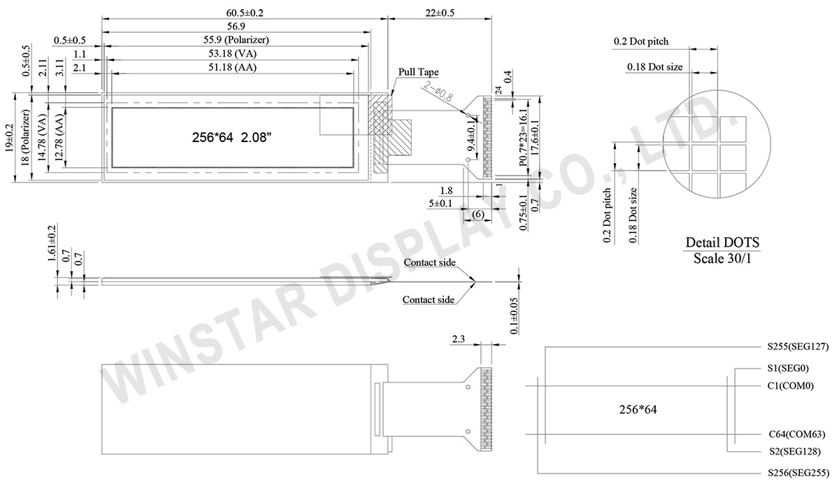
WEO025664A with Hotbar FPC
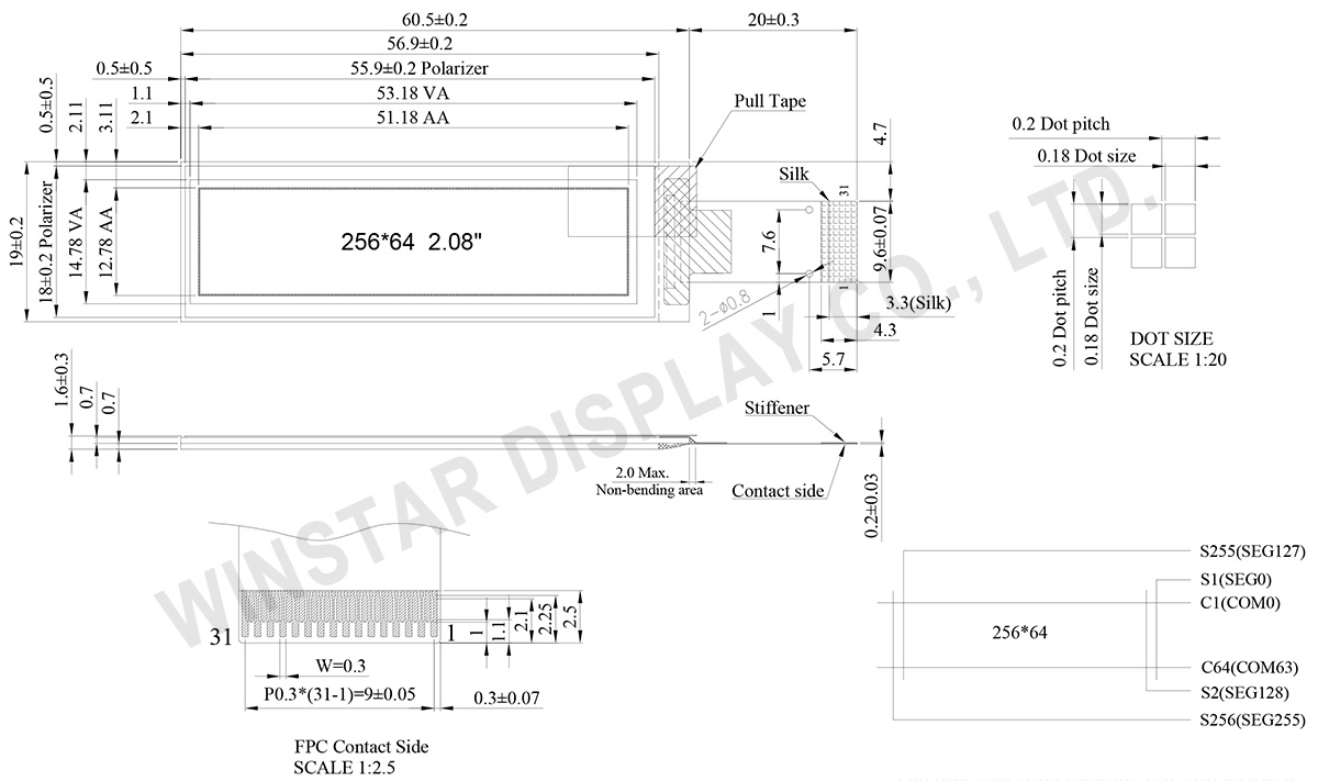
WEO025664A with ZIF FPC
Data source ref: WEO025664ALAP3N00000
Технические характеристики
Функции контроллера контактного интерфейса
| No. | Символы | Описание | ||||||||||||
|---|---|---|---|---|---|---|---|---|---|---|---|---|---|---|
| 1 | VCC | Power supply for panel driving voltage. This is also the most positive power voltage supply pin. It is supplied by external high voltage source. | ||||||||||||
| 2 | VP | This pin is the segment pre-charge voltage reference pin. A capacitor should be connected between this pin and VSS. No external power supply is allowed to connect to this pin. |
||||||||||||
| 3 | VCOMH | COM signal deselected voltage level. A capacitor should be connected between this pin and VSS. No external power supply is allowed to connect to this pin. |
||||||||||||
| 4 | VDD | Power supply for core logic operation. VDD can be supplied externally (within the range of 1.65V to 2.6V) or regulated internally from VCI when VCI is >2.6V. A capacitor should be connected between VDD and VSS under all circumstances. |
||||||||||||
| 5 | IREF | This pin is the segment output current reference pin. When external IREF is used, a resistor should be connected between this pin and VSS to maintain current of around 18.75uA. When internal IREF is used, this pin should be kept NC. |
||||||||||||
| 6 | VSS | Ground pin. It must be connected to external ground. | ||||||||||||
| 7 | VSS | Ground pin. It must be connected to external ground. | ||||||||||||
| 8 | VCI | Low voltage power supply. VCI must always be equal to or higher than VDD and VDDIO. |
||||||||||||
| 9 | BS0 | MCU bus interface selection pins. Select appropriate logic setting as described in the following table. BS2 and BS1, BS0 are pin select.
|
||||||||||||
| 10 | BS1 | |||||||||||||
| 11 | BS2 | |||||||||||||
| 12 | CS | This pin is the chip select input connecting to the MCU. The chip is enabled for MCU communication only when CS is pulled LOW (active LOW). In I2C mode, this pin must be connected to VSS. |
||||||||||||
| 13 | RES | This pin is reset signal input. When the pin is pulled LOW, initialization of the chip is executed. Keep this pin pull HIGH during normal operation. |
||||||||||||
| 14 | D/C | This pin is Data/Command control pin connecting to the MCU. When the pin is pulled HIGH, the data at D[7:0] will be interpreted as data. When the pin is pulled LOW, the data at D[7:0] will be transferred to a command register. In I2C mode, this pin acts as SA0 for slave address selection. When 3-wire serial interface is selected, this pin must be connected to VSS. |
||||||||||||
| 15 | R/W | This pin is read / write control input pin connecting to the MCU interface. When 6800 interface mode is selected, this pin will be used as Read/Write (R/W) selection input. Read mode will be carried out when this pin is pulled HIGH and write mode when LOW. When 8080 interface mode is selected, this pin will be the Write (WR) input. Data write operation is initiated when this pin is pulled LOW and the chip is selected. When serial or I2C interface is selected, this pin must be connected to VSS. |
||||||||||||
| 16 | RD | This pin is MCU interface input. When 6800 interface mode is selected, this pin will be used as the Enable signal. Read/write operation is initiated when this pin is pulled HIGH and the chip is selected. When 8080 interface mode is selected, this pin receives the Read (RD) signal. Read operation is initiated when this pin is pulled LOW and the chip is selected. When serial or I2C interface is selected, this pin must be connected to VSS. |
||||||||||||
| 17 | D0 | These pins are bi-directional data bus connecting to the MCU data bus. Unused pins are recommended to tie LOW. When serial interface mode is selected, D0 will be the serial clock input: SCLK; D1 will be the serial data input: SID. When I2C mode is selected, D2, D1 should be tied together and serve as SDAout, SDAin in application and D0 is the serial clock input, SCL. |
||||||||||||
| 18 | D1 | |||||||||||||
| 19 | D2 | |||||||||||||
| 20 | D3 | |||||||||||||
| 21 | D4 | |||||||||||||
| 22 | D5 | |||||||||||||
| 23 | D6 | |||||||||||||
| 24 | D7 |
Механические характеристики
| Наименование | Измерения | Единица |
|---|---|---|
| Разрешение | 256 x 64 | точек |
| Габариты | 60.5 x 19.0 x 1.61 | mm |
| Активная область | 51.18 x 12.78 | mm |
| Размер пикселя | 0.18 x 0.18 | mm |
| Шаг пикселя | 0.2 x 0.2 | mm |
| Матрица | Пассивная | |
| Цвет дисплея | монохромные | |
| Рабочий цикл | 1/64 Duty | |
| Gray Scale | 4 Bits | |
| IC | SSD1362 | |
| Интерфейс | 3-Wire and 4-Wire SPI, I2C, 6800, 8080 | |
| Диагональ | 2.08 дюйма | |
Абсолютные максимальные значения
| Параметр | Символы | Минимальный | Максимальный | Единица |
|---|---|---|---|---|
| Supply Voltage for Operation | VCI | -0.5 | 5.5 | V |
| Supply Voltage for Logic | VDD | -0.5 | 2.75 | V |
| Supply Voltage for Display | VCC | -0.5 | 21 | V |
| Operating Temperature | TOP | -40 | 80 | °C |
| Storage Temperature | TSTG | -40 | 85 | °C |
Электронные характеристики
DC Электронные характеристики
| Наименование | Символы | Кондиция | Минимальный | Типичный | Максимальный | Единица |
|---|---|---|---|---|---|---|
| Supply Voltage for Logic | VCI | - | 2.8 | 3.0 | 3.3 | V |
| Supply Voltage for Display | VCC | - | 11.5 | 12 | 12.5 | V |
| Input High Volt. | VIH | - | 0.8×VCI | - | VCI | V |
| Input Low Volt. | VIL | - | VSS | - | 0.2×VCI | V |
| Output High Volt. | VOH | - | 0.9×VCI | - | VCI | V |
| Output Low Volt. | VOL | - | VSS | - | 0.1×VCI | V |
| 50% Check Board operating Current | ICC | VCC=12V | - | 15 | 30 | mA |
FPC Options:
| Drawing | FPC Length | PIN | Pitch | ZIF or HOTBAR FPC | Interface | FPC No. | Create Date |
|---|---|---|---|---|---|---|---|
 |
23 | 24 | 0.7 | HOTBAR | 3-Wire and 4-Wire SPI, I2C, 6800, 8080 | FPC2070002401XXXXX02 | 20180611 |
 |
21 | 31 | 0.3 | ZIF | 3-Wire and 4-Wire SPI, I2C, 6800, 8080 | FPC2030003111XXXXX02 | 20171107 |
