


우리는 귀하의 프라이버시를 소중히 여깁니다
"모든 쿠키 허용"을 클릭하면 사이트 탐색을 개선하고, 사이트 사용을 분석하며, 마케팅 및 성능 노력에 도움을 주기 위해 쿠키를 귀하의 장치에 저장하는 데 동의한 것으로 간주됩니다. 이 주제에 대한 추가 정보는 당사의 정책에서 확인할 수 있습니다. 개인정보 보호정책


| Pin No. | 기호 | Level | 설명 | ||||||||||||
|---|---|---|---|---|---|---|---|---|---|---|---|---|---|---|---|
| 1 | PSB | I | PSB selects the interface type: Serial or Parallel. | ||||||||||||
| 2 | C86 | I | C86 selects the microprocessor type in parallel interface mode.
|
||||||||||||
| 3 | VG | Power | VG is the LCD driving voltage for segment circuits. | ||||||||||||
| 4 | XV0 | Power | XV0 is the LCD driving voltage for common circuits at positive frame. | ||||||||||||
| 5 | V0 | Power | V0 is the LCD driving voltage for common circuits at negative frame. | ||||||||||||
| 6 | VSS | Power | This is a 0V terminal connected to the system GND. | ||||||||||||
| 7 | VDD | Power | Shared with the MPU power supply terminal VDD. ( 3.3 V ) | ||||||||||||
| 8-15 | D7-D0 | I/O | When using 8-bit parallel interface: (6800 or 8080 mode) 8-bit bi-directional data bus. Connect to the data bus of 8-bit microprocessor. When CSB is non-active (CSB=“H”), D[7:0] pins are high impedance. |
||||||||||||
| I | When using serial interface: 4-LINE D7=SDA : Serial data input. D6=SCL : Serial clock input. D[5:0] are not used and should connect to “H” by VDD1 or VDDH. When CSB is non-active (CSB=“H”), D[7:0] pins are high impedance. |
||||||||||||||
| 16 | ERD | I | Read/Write execution control pin. When PSB is “H”,
|
||||||||||||
| 17 | RWR | I | Read/Write execution control pin. When PSB is “H”,
|
||||||||||||
| 18 | A0 | I | It determines whether the access is related to data or command. A0=“H” : Indicates that signals on D[7:0] are display data. A0=“L” : Indicates that signals on D[7:0] are command. |
||||||||||||
| 19 | RSTB | I | Hardware reset input pin. When RSTB is “L”, internal initialization is executed and the internal registers will be initialized. | ||||||||||||
| 20 | CSB | I | Chip select input pin. Interface access is enabled when CSB is “L”.When CSB is non-active (CSB=“H”), D[7:0] pins are high impedance. |
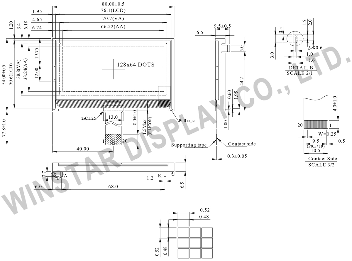
| 항목 | 치수 | 단위 |
|---|---|---|
| 점의 수 | 128 x 64 | - |
| 모듈 치수 | 80.0 x 54.0 x 9.5 | mm |
| 보기 영역 | 70.7 x 38.8 | mm |
| 활성 영역 | 66.52 x 33.24 | mm |
| 도트 크기 | 0.48 x 0.48 | mm |
| 도트 피치 | 0.52 x 0.52 | mm |
| 듀티 | 1/64 , 1/9 Bias | |
| 역광 타입 | LED | |
| IC | ST7567 | |
| 인터페이스 | 6800/8080/4-Line SPI | |
| 항목 | 기호 | 최소값 | 대표값 | 최대값 | 단위 |
|---|---|---|---|---|---|
| 작동 온도 | TOP | -20 | - | +70 | ℃ |
| 보관 온도 | TST | -30 | - | +80 | ℃ |
| 입력 전압 | VI | -0.3 | - | VDD+0.3 | V |
| Digital Power Supply Voltage | VDD,VSS | -0.3 | - | 3.6 | V |
| LCD Power supply voltage | V0-XV0 | -0.3 | - | 16 | V |
| 항목 | 기호 | 조건 | 최소값 | 대표값 | 최대값 | 단위 |
|---|---|---|---|---|---|---|
| Supply Voltage For Logic | VDD-VSS | - | 3.0 | 3.3 | 3.6 | V |
| Supply Voltage For LCM | XV0-V0 | Ta=-20℃ Ta=25℃ Ta=70℃ |
- - - |
- 10.0 - |
- - - |
V V V |
| Input High Volt. | VIH | - | 0.7 VDD | - | VDD | V |
| Input Low Volt. | VIL | - | VSS | - | 0.3VDD | V |
| Output High Volt. | VOH | - | 0.8VDD | - | VDD | V |
| Output Low Volt. | VOL | - | VSS | - | 0.2VDD | V |
| Supply Current(No include LED Backlight) | IDD | - | - | 2.0 | - | mA |

"모든 쿠키 허용"을 클릭하면 사이트 탐색을 개선하고, 사이트 사용을 분석하며, 마케팅 및 성능 노력에 도움을 주기 위해 쿠키를 귀하의 장치에 저장하는 데 동의한 것으로 간주됩니다. 이 주제에 대한 추가 정보는 당사의 정책에서 확인할 수 있습니다. 개인정보 보호정책