| Pin No. |
Símbolo |
Level |
Descripción |
| 1 |
/CS1 |
|
This is the chip select signal. When /CS1 = “L” , then the
chip select becomes active, and data/command I/O is enabled. |
| 2 |
/RES |
|
When /RES is set to “L” , the settings are initialized. |
| 3 |
A0 |
|
This is connect to the least significant bit of the normal MPU address bus, and it determines whether the data bits are data or a command.
A0 = “H”: Indicates that D0 to D7 are display data.
A0 = “L”: Indicates that D0 to D7 are control data. |
| 4 |
/WR(R/W) |
|
When connected to an 8080 MPU, this is active LOW.
(R/W) This terminal connects to the 8080 MPU /WR signal. The signals on the data bus are latched at the rising edge of the /WR signal.
When connected to a 6800 Series MPU:
This is the read/write control signal input terminal.
When R/W = “H”: Read.
When R/W = “L”: Write. |
| 5 |
/RD(E) |
|
When connected to an 8080 MPU, this is active LOW.
(E) This pin is connected to the /RD signal of the 8080 MPU, and the ST7565P series data bus is in an output status when this signal is “L”.
When connected to a 6800 Series MPU, this is active HIGH.
This is the 6800 Series MPU enable clock input terminal. |
| 6 |
DB0 |
|
This is an 8-bit bi-directional data bus that connects to an 8-bit or 16-bit standard MPU data
Bus. |
| 7 |
DB1 |
|
| 8 |
DB2 |
|
| 9 |
DB3 |
|
| 10 |
DB4 |
|
| 11 |
DB5 |
|
| 12 |
DB6 |
|
| 13 |
DB7 |
|
| 14 |
VDD |
|
Shared with the MPU power supply terminal VDD. ( 3.3 V ) |
| 15 |
VSS |
|
This is a 0V terminal connected to the system GND. |
| 16 |
VOUT |
|
DC/DC voltage converter. Connect a capacitor between this terminal and VSS. |
| 17 |
CAP5+ |
|
DC/DC voltage converter. Connect a capacitor between this terminal and the CAP1- terminal. |
| 18 |
CAP3+ |
|
DC/DC voltage converter. Connect a capacitor between this terminal and the CAP1- terminal. |
| 19 |
CAP1- |
|
DC/DC voltage converter. Connect a capacitor between this terminal and the CAP1+ terminal. |
| 20 |
CAP1+ |
|
DC/DC voltage converter. Connect a capacitor between this terminal and the CAP1- terminal. |
| 21 |
CAP2+ |
|
DC/DC voltage converter. Connect a capacitor between this terminal and the CAP2- terminal. |
| 22 |
CAP2- |
|
DC/DC voltage converter. Connect a capacitor between this terminal and the CAP2+ terminal. |
| 23 |
CAP4+ |
|
DC/DC voltage converter. Connect a capacitor between this terminal and the CAP2- terminal. |
| 24 |
VRS |
|
This is the externally-input VREG power supply for the LCD power supply voltage regulator. |
| 25 |
V4 |
|
This is a multi-level power supply for the liquid crystal drive. The voltage Supply applied is determined by the liquid crystal cell, and is changed through the use of a resistive voltage divided or through changing the impedance using an op. amp.
Voltage levels are determined based on Vss, and must maintain the relative magnitudes shown below.
V0 ≧V1 ≧V2 ≧V3 ≧V4 ≧Vss
When the power supply turns ON, the internal power supply circuits produce the V1 to V4 voltages shown below. The voltage settings are selected using the LCD bias set command.
 |
| 26 |
V3 |
|
| 27 |
V2 |
|
| 28 |
V1 |
|
| 29 |
V0 |
|
| 30 |
VR |
|
Output voltage regulator terminal. Provides the voltage between VDD and V5 through a resistive voltage divider.
IRS = “L” : the V5 voltage regulator internal resistors are not used .
IRS = “H” : the V5 voltage regulator internal resistors are used . |
| 31 |
C86 |
|
This is the MPU interface switch terminal.
C86 = “H”: 6800 Series MPU interface.
C86 = “L”: 8080 MPU interface. |
| 32 |
P/S |
|
This is the parallel data input/serial data input switch terminal.
P/S = “H”: Parallel data input.
P/S = “L”: Serial data input.
The following applies depending on the P/S status:
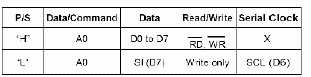
When P/S = “L”, D0 to D5 may be “H”, “L” or Open.
RD (E) and WR (R/W) are fixed to either “H” or “L”.
With serial data input, It is impossible read data from RAM . |
| 33 |
/HPM |
|
This is the power control terminal for the power supply circuit for liquid crystal drive.
HPM = “H”: Normal mode
HPM = “L”: High power mode |
| 34 |
IRS |
|
This terminal selects the resistors for the V5 voltage level adjustment.
IRS = “H”: Use the internal resistors
IRS = “L”: Do not use the internal resistors. The V5 voltage level is regulated by an external resistive voltage divider attached to the VR terminal |