Startseite Produkte TFT-LCDs Standard TFT LCD Modul WF24MTLAJDNT0

240x320 SPI TFT Module 2,4 Zoll mit Resistive Touch Screen

Modellnummer WF24MTLAJDNT0

►Größe: 2,4 Zoll
►Auflösung: 240 x 320 Punkten
►Betrachtungsrichtung: 6H
►Schnittstelle: SPI
►Treiber IC:ST7789V
►Steuerplatine: Nein
►Helligkeit (cd/m²): 350
►Durchsteckrahmen: Nein
►Touchscreen: Resistiven Touchscreen (RTP)

Beschreibung

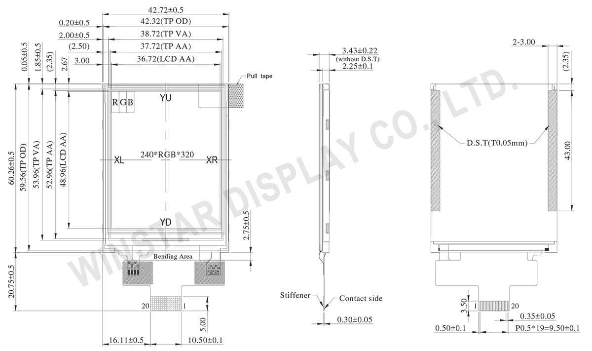
WF24MTLAJDNT0 ist ein vollfarbiges 2,4 zoll TFT-Display-Modul mit resistivem Touchscreen und hat eine Auflösung von 240 x 320. Das Modell WF24MTLAJDNT0 hat eine Modulgröße von 42,72 × 60,26 mm und eine aktive Fläche von 36,72 × 48,96 mm. Dieses Modul ist mit IC ST7789V bestückt, unterstützt 4-adrige -SPI serielle Schnittstelle.

Das Panel dieses Modul besitzt eine blendfreier Oberfläche bei Blickrichtung nach oben (6 Uhr) und Graustufeninversion bei Blickrichtung nach unten (12 Uhr). Die 6-Uhr-Blickrichtung dieses 2,8-Zoll-TFT-LCD-Moduls eignet sich gut für Geräte, die oberhalb der Augenhöhe unverblasst abgelesen werden, z. B. Signalmessgeräte oder Labortischgeräte, Hand-Mikroskope und andere Handgeräte.

Dieses 2,4" TFT hat eine Helligkeit von bis zu 350 cd/m2 (typischer Wert) und ein Kontrastverhältnis von 500:1 (üblicher Wert). Die Versorgungsspannung für die Analogschaltungen ist von 2,4 V und 3,6 V (üblicher Wert 3,3 V). Es kann bei Temperaturen von -20 ℃ bis + 70 ℃ betrieben werden; die Lagertemperatur liegt zwischen -30 ° C und + 80 ° C. Dieses 2,4" TFT-LCD ist hochformatig. Wenn Sie den Querformatmodus verwenden möchten, kontaktieren Sie uns bitte für mehr technischen Support.

Zeichnung

SPI TFT Display, SPI TFT LCD, SPI LCD Display, SPI Display Module - WF24MTLAJDNT0

Technische Daten

Schnittstelle

LCM PIN Definition

NO Symbol Function
1 GND Ground
2 VLED+ Anode of LED backlight.
3 VLED- Cathode of LED backlight.
4 GND Ground
5 VCC Power supply
6 RESET System reset pin. (RESX)
signal is active low
7 SDA When IM3: Low, SPI interface input/output pin.
When IM3: High, SPI interface input pin.
The data is latched on the rising edge of the SCL signal.
If not used, please fix this pin at VDDI or DGND level.
8 DCX(SCL) This pin is used to be serial interface clock.
DCX=’1’: display data or parameter.
DCX=’0’: command data.
If not used, please fix this pin at VDDI or DGND.
9 CSX Chip selection pin
Low enable.
High disable.
10 WRX(D/CX) Display data/command selection pin in 4-line serial interface.
Second Data lane in 2 data lane serial interface.
If not used, please fix this pin at VDDI or DGND.
11 GND Ground
12 SDO(DOUT) SPI interface output pin.
The data is output on the falling edge of the SCL signal.
If not used, let this pin open.
13 TE Tearing effect signal is used to synchronize MCU to frame memory
writing.
If not used, please let this pin open
14 IM3 The MCU interface mode select.
IM3 IM2 IM1 IM0 MPU Interface Mode Data pin
0 1 1 0 4-line 8bit serial I/F SDA: in/out
1 1 1 0 4-line 8bit serial I/F II SDA: in/SDO: out
15 GND Ground
16 XR Right electrode
17 YD Bottom electrode
18 XL Left electrode
19 YU Top electrode
20 GND Ground

Allgemeine Spezifikationen

Artikel Ausmaß Einheit
Größe 2,4 Zoll
Punktmatrix 240 × RGB × 320(TFT) dots
Abmaße der modul 42,72(W) × 60,26(H) × 3,43(D) mm
Aktiver Bereich 36,72 × 48,96 mm
Punktabstand 0,153 × 0,153 mm
LCD Typ TFT, Weiß, Transmissiv
Schnittstelle SPI
TFT Driver IC ST7789V oder gleichwertig
Betrachtungsrichtung 6 o'clock
Grauskala-Umkehrrichtung 12 o'clock
Seitenverhältnis Portrait
Hintergrundbeleuchtung Typ LED, Weiß
Touchscreen Resistiven Touchscreen
Oberfläche Anti-Reflextion

absolute Grenzwerte

Artikel Symbol Mindestwert typischer Wert Maximalwert Einheit
Betriebstemperatur TOP -20 +70
Lagertemperatur TST -30 +80

elektrische Eigenschaften

Artikel Symbol Bedingung Mindestwert typischer Wert Maximalwert Einheit
Supply Voltage For Analog Vcc 2,4 3,3 3,6 V
Supply Current For LCM Icc 6,4 9,6 mA
go top
close