


产品叙述
WEO012864G是最多任务控产品应用所采用的COG OLED显示器模块,尺寸2.42英寸。我们推出此款带电容式触控面板(CTP)型号供客户选用,面板分辨率128x64点,内置SSD1309 IC,支援 6800/8080 8-bit 并行接口,I2C与4-线SPI接口,3V电压驱动,1/64 duty。WEO012864G电容式触控面板内建GT911 IC,支持I2C接口,单点触控。此OLED模块具有10,000:1的高对比度度,影像显示更清晰。
此款含电容触控面板模块是COG结构OLED,非常适用于智能家电、智能检测、能源系统、量测仪器、POS系统、智能医疗设备等产品。模块工作温度是-20℃至 70℃,储存温度-30℃至 80℃。
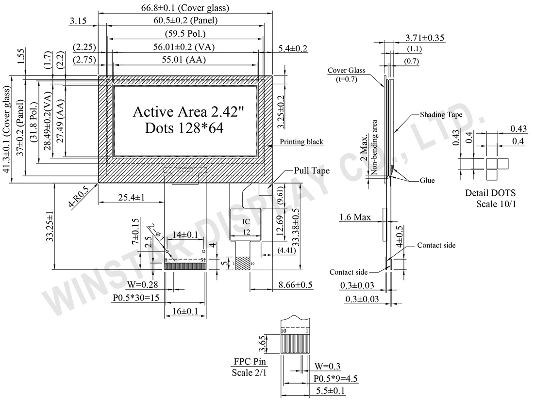
规格图
Data source ref: WEO012864GWPP3D00000
产品规格
Pin功能定义
| No. | 符号 | 说明 | |||||||||||||||
|---|---|---|---|---|---|---|---|---|---|---|---|---|---|---|---|---|---|
| 1 | NC(GND) | No connection | |||||||||||||||
| 2 | VSS | Ground. | |||||||||||||||
| 3-10 | NC | No connection | |||||||||||||||
| 11 | VDD | Power supply pin for core logic operation | |||||||||||||||
| 12 | BS1 | MCU bus interface selection pins. Select appropriate logic setting as described in the following table. BS2, BS1 and BS0 are pin select
(1) 0 is connected to VSS (2) 1 is connected to VDD |
|||||||||||||||
| 13 | BS2 | ||||||||||||||||
| 14 | NC | No connection | |||||||||||||||
| 15 | CS# | This pin is the chip select input connecting to the MCU. The chip is enabled for MCU communication only when CS# is pulled LOW (active LOW). |
|||||||||||||||
| 16 | RES# | This pin is reset signal input. When the pin is pulled LOW, initialization of the chip is executed. Keep this pin pull HIGH during normal operation. |
|||||||||||||||
| 17 | D/C# | This pin is Data/Command control pin connecting to the MCU. When the pin is pulled HIGH, the data at D[7:0] will be interpreted as data. When the pin is pulled LOW, the data at D[7:0] will be transferred to a command register. In I2C mode, this pin acts as SA0 for slave address selection. |
|||||||||||||||
| 18 | R/W# | This pin is read / write control input pin connecting to the MCU interface. When 6800 interface mode is selected, this pin will be used as Read/Write (R/W#) selection input. Read mode will be carried out when this pin is pulled HIGH and write mode when LOW. When 8080 interface mode is selected, this pin will be the Write (WR#) input. Data write operation is initiated when this pin is pulled LOW and the chip is selected. When serial or I2C interface is selected, this pin must be connected to VSS. |
|||||||||||||||
| 19 | E/RD# | This pin is MCU interface input. When 6800 interface mode is selected, this pin will be used as the Enable (E) signal. Read/write operation is initiated when this pin is pulled HIGH and the chip is selected. When 8080 interface mode is selected, this pin receives the Read (RD#) signal. Read operation is initiated when this pin is pulled LOW and the chip is selected. When serial or I2C interface is selected, this pin must be connected to VSS. |
|||||||||||||||
| 20~27 | D0~D7 | These pins are bi-directional data bus connecting to the MCU data bus. Unused pins are recommended to tie LOW. When serial interface mode is selected, D0 will be the serial clock input: SCLK; D1 will be the serial data input: SDIN and D2 should be kept NC. When I2C mode is selected, D2, D1 should be tied together and serve as SDAout, SDAin in application and D0 is the serial clock input, SCL. |
|||||||||||||||
| 28 | IREF | This pin is the segment output current reference pin. IREF is supplied externally. |
|||||||||||||||
| 29 | VCOMH | COM signal deselected voltage level. A capacitor should be connected between this pin and VSS. |
|||||||||||||||
| 30 | VCC | Power supply for panel driving voltage. This is also the most positive power voltage supply pin. | |||||||||||||||
| 31 | NC(GND) | No connection |
CTP PIN Definition
| No. | 符号 | 说明 |
|---|---|---|
| 1 | GND | Power ground |
| 2 | VDD | Power supply |
| 3 | INT | Interrupt signal, active low, asserted to request Host start a new transaction |
| 4 | SDA | I2C data signal |
| 5 | SCL | I2C clock signal |
| 6 | RST | External reset signal, active low |
| 7 | GND | Power ground |
| 8 | GND | Power ground |
| 9 | GND | Power ground |
| 10 | GND | Power ground |
规格说明
| 项目 | 规格 | 单位 |
|---|---|---|
| 点阵(分辨率) | 128 x 64 | Dot |
| 模块尺寸 | 66.8 × 41.3 × 3.71 | mm |
| 有效区域 | 55.01 × 27.49 | mm |
| 点大小 | 0.40 × 0.40 | mm |
| 点间距 | 0.43 × 0.43 | mm |
| 显示模式 | 被动矩阵 | |
| 发光颜色 | 单色 | |
| 接口 | 8Bits 68xx 80xx / 4线 SPI / I2C | |
| 驱动方式 | 1/64 Duty | |
| OLED IC | SSD1309 | |
| 尺寸 | 2.42 寸 | |
| CTP IC | GT911 | |
| 支援手指数 | 1 | |
| CTP接口 | I2C | |
| 表面 | 亮面 | |
最大绝对额定值
最大绝对额定值
| 参数 | 符号 | 最小值 | 最大值 | 单位 |
|---|---|---|---|---|
| 逻辑电源电压 | VDD | -0.3 | 4 | V |
| 显示电源电压 | VCC | 0 | 15 | V |
| 工作温度 | TOP | -20 | +70 | °C |
| 储存温度 | TSTG | -30 | +80 | °C |
触控面板控制器 GT911
| 参数 | 符号 | 最小值 | 最大值 | 单位 |
|---|---|---|---|---|
| 电源电压 | VDD | 2.66 | 3.47 | V |
电气特性
DC 电器特性
| 项目 | 符号 | 条件 | 最小值 | 典型值 | 最大值 | 单位 |
|---|---|---|---|---|---|---|
| 逻辑电源电压 | VDD | - | 2.8 | 3.0 | 3.3 | V |
| 显示电源电压 | VCC | - | 12.5 | 13.0 | 13.5 | V |
| 输入高准位 | VIH | - | 0.8×VDD | - | - | V |
| 输入低准位 | VIL | - | - | - | 0.2×VDD | V |
| 输出高准位 | VOH | - | 0.9×VDD | - | - | V |
| 输出低准位 | VOL | - | - | - | 0.1×VDD | V |
| 50%显示画面耗电流 | VCC =13.0V | - | 25 | 36 | mA | |
触控面板控制器 GT911
| 项目 | 符号 | 最小值 | 典型值 | 最大值 | 单位 |
|---|---|---|---|---|---|
| 电源电压 | VDD | 2.8 | 3.0 | 3.3 | V |
| 输入高电压 | VIH | 0.75xVDD | VDD+0.3 | V | |
| 输入低电压 | VIL | -0.3 | - | 0.25xVDD | V |
| 输出高电压 | VOH | 0.85xVDD | - | - | V |
| 输出低电压 | VOL | - | - | 0.15xVDD | V |
