


产品叙述
WEO012864AB是双色OLED显示模块,模块为0.96寸绘图型COG结构OLED显示器,由128x64点阵组成显示画面,标准发光色为黄色和天空蓝。此型号内置SSD1315 IC,支持I2C,3/4线SPI,以及8-bit 6800/8080并列接口,驱动方式1/64 duty。WEO012864AB型号是WEO012864M型号IC替代方案;WEO012864AB的面板边框比WEO012864M窄,但电气特性和PFC引脚定义相同。客户只需调整初始代码。此型号OLED模块可支持内部升压及外部供电。
此双色OLED模块适何运用在医疗设备,尤其是血氧机等。WEO012864AB模块可在-30℃~+70℃温度下工作;储存温度范围为-30℃~+70℃。
规格图
Data source of: WEO012864ABXPP3N0Y000
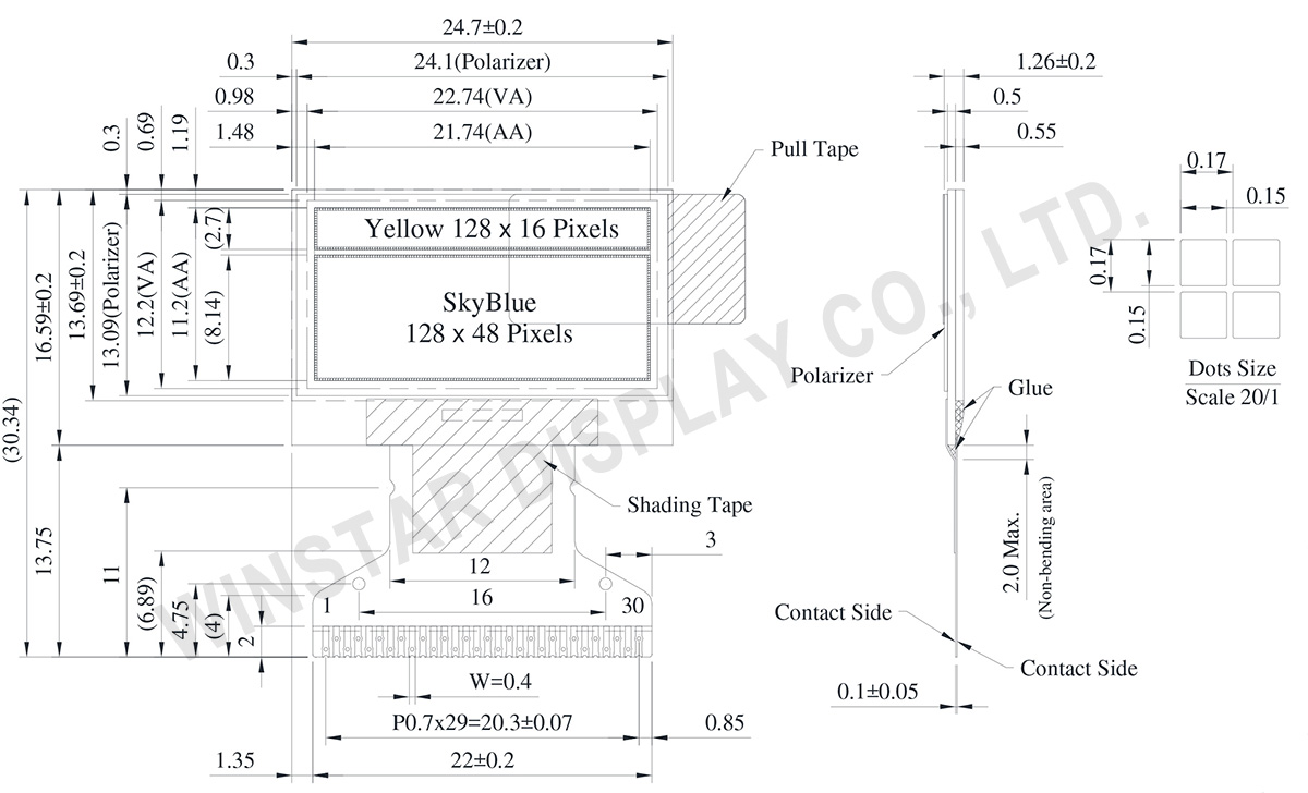
产品规格
Pin功能定义
| No. | 符号 | 功能说明 | ||||||||||||||||||||||||
|---|---|---|---|---|---|---|---|---|---|---|---|---|---|---|---|---|---|---|---|---|---|---|---|---|---|---|
| 1 | N.C. (GND) | The supporting pins can reduce the influences from stresses on the function pins. These pins must be connected to external ground. | ||||||||||||||||||||||||
| 2 | C2P | C1P/C1N – Pin for charge pump capacitor; Connect to each other with a capacitor. C2P/C2N – Pin for charge pump capacitor; Connect to each other with a capacitor. |
||||||||||||||||||||||||
| 3 | C2N | |||||||||||||||||||||||||
| 4 | C1P | |||||||||||||||||||||||||
| 5 | C1N | |||||||||||||||||||||||||
| 6 | VBAT | This is the power supply pin for the internal buffer of the DC/DC voltage converter. It must be connected to external source when the converter is used. It should be connected to VDD when the converter is not used. | ||||||||||||||||||||||||
| 7 | NC | NC | ||||||||||||||||||||||||
| 8 | VSS | This is a ground pin. | ||||||||||||||||||||||||
| 9 | VDD | Power supply pin for core logic operation. | ||||||||||||||||||||||||
| 10 | BS0 | These pins are MCU interface selection input. See the following table:
|
||||||||||||||||||||||||
| 11 | BS1 | |||||||||||||||||||||||||
| 12 | BS2 | |||||||||||||||||||||||||
| 13 | CS# | This pin is the chip select input connecting to the MCU. The chip is enabled for MCU communication only when CS# is pulled LOW (active LOW). |
||||||||||||||||||||||||
| 14 | RES# | This pin is reset signal input. When the pin is low, initialization of the chip is executed. Keep this pin HIGH (i.e. connect to VDD) during normal operation. | ||||||||||||||||||||||||
| 15 | D/C# | This pin is Data/Command control pin connecting to the MCU. When the pin is pulled HIGH, the data at D[7:0] will be interpreted as data. When the pin is pulled LOW, the data at D[7:0] will be transferred to a command register. In I2C mode, this pin acts as SA0 for slave address selection. When 3-wire serial interface is selected, this pin must be connected to VSS. |
||||||||||||||||||||||||
| 16 | R/W# | This is read / write control input pin connecting to the MCU interface. When interfacing to a 6800-series microprocessor, this pin will be used as Read/Write (R/W#) selection input. Read mode will be carried out when this pin is pulled HIGH (i.e. connect to VDD) and write mode when LOW. When 8080 interface mode is selected, this pin will be the Write (WR#) input. Data write operation is initiated when this pin is pulled LOW and the chip is selected. When serial or I2C interface is selected, this pin must be connected to VSS. |
||||||||||||||||||||||||
| 17 | E/RD# | This pin is MCU interface input. When 6800 interface mode is selected, this pin will be used as the Enable (E) signal. Read/write operation is initiated when this pin is pulled HIGH and the chip is selected. When 8080 interface mode is selected, this pin receives the Read (RD#) signal. Read operation is initiated when this pin is pulled LOW and the chip is selected. When serial or I2C interface is selected, this pin must be connected to VSS. |
||||||||||||||||||||||||
| 18~25 | D0~D7 | These pins are bi-directional data bus connecting to the MCU data bus. Unused pins are recommended to tie LOW. When serial interface mode is selected, D2 should be either tied LOW or tied together with D1 as the serial data input: SDIN, and D0 will be the serial clock input: SCLK. When I2C mode is selected, D2, D1 should be tied together and serve as SDAout, SDAin in application and D0 is the serial clock input, SCL. |
||||||||||||||||||||||||
| 26 | IREF | When external IREF is used, a resistor should be connected between this pin and VSS to maintain the IREF current at a maximum of 30uA. When internal IREF is used, this pin should be kept NC. |
||||||||||||||||||||||||
| 27 | VCOMH | COM signal deselected voltage level. A capacitor should be connected between this pin and VSS. |
||||||||||||||||||||||||
| 28 | VCC | Power supply for panel driving voltage. This is also the most positive power voltage supply pin. When charge pump is enabled, a capacitor should be connected between this pin and VSS. |
||||||||||||||||||||||||
| 29 | VLSS | This is an analog ground pin. It should be connected to VSS externally. | ||||||||||||||||||||||||
| 30 | NC (GND) |
The supporting pins can reduce the influences from stresses on the function pins. These pins must be connected to external ground. |
规格说明
| 项目 | 尺寸 | 单位 |
|---|---|---|
| 点阵 | 128 × 64 Dots | - |
| 模块尺寸 | 24.7 × 16.59 × 1.26 | mm |
| 有效区域 | 21.74 × 11.20 | mm |
| 点间距 | 0.15 × 0.15 | mm |
| 点大小 | 0.17 × 0.17 | mm |
| 显示模式 | 被动矩阵 | |
| 发光颜色 | 双色 (黄色 / 天空蓝) | |
| 驱动方式 | 1/64 Duty | |
| IC | SSD1315 | |
| 接口 | 6800,8080,SPI,I2C | |
| 尺寸 | 0.96 寸 | |
最大绝对额定值
| 参数 | 符号 | 最小值 | 最大值 | 单位 |
|---|---|---|---|---|
| 逻辑电源电压 | VDD | 0 | 4 | V |
| 电荷帮浦稳压器电源电压 | VBAT | -0.3 | 6.0 | V |
| 显示电源电压 | VCC | 0 | 18.0 | V |
| 工作温度 | TOP | -30 | +70 | °C |
| 储存温度 | TSTG | -30 | +70 | °C |
电气特性
DC 电气特性
| 项目 | 符号 | 条件 | 最小值 | 典型值 | 最大值 | 单位 |
|---|---|---|---|---|---|---|
| 逻辑电源电压 | VDD | - | 1.65 | 3.0 | 3.3 | V |
| 显示电源电压 (Supplied Externally) |
VCC | - | 7.5 | 8.0 | 8.5 | V |
| 电荷帮浦稳压器电源电压 | VBAT | - | 3.0 | 3.5 | 4.2 | V |
| 显示器的电荷帮浦输出电压 (Generated by Internal DC/DC) | Charge Pump VCC |
- | 7.0 | 7.5 | - | V |
| 输入高电压 | VIH | - | 0.8×VDD | - | VDD | V |
| 输入低电压 | VIL | - | 0 | - | 0.2×VDD | V |
| 输出高电压 | VOH | - | 0.9×VDD | - | VDD | V |
| 输出低电压 | VOL | - | 0 | - | 0.1×VDD | V |
| VCC的工作电流 (Display 50% Pixel on) (VCC Supplied Externally) |
ICC | VCC =8V | - | 5.0 | 7.5 | mA |
| 50%显示画面耗电流 (VCC Generated by Internal DC/DC) | IBAT | VBAT=3.5V | - | 15 | 22.5 | mA |
Search keyword: 128x64 oled, oled 128x64, 0.96 oled, 0.96" oled, 0.96 inch oled, oled 0.96, oled 0.96", 0.96寸oled, oled 0.96寸
