


产品叙述
WEO006448B 这是一款0.66吋小尺寸消费性规格 COG OLED显示器模块,分辨率为64x48点阵。此OLED模块使用3V电压驱动,并支持多种传输接口4线SPI串行接口:6800、8080、I2C接口,显示50% Checkboard电流为3mA @7.5V VCC(典型值)。此型号OLED模块可支持内部升压及外部供电。
WEO006448B 模块适用于可穿戴设备、便携式设备等,工作温度为–30℃至+70℃,储存温度为-30℃至+70℃。
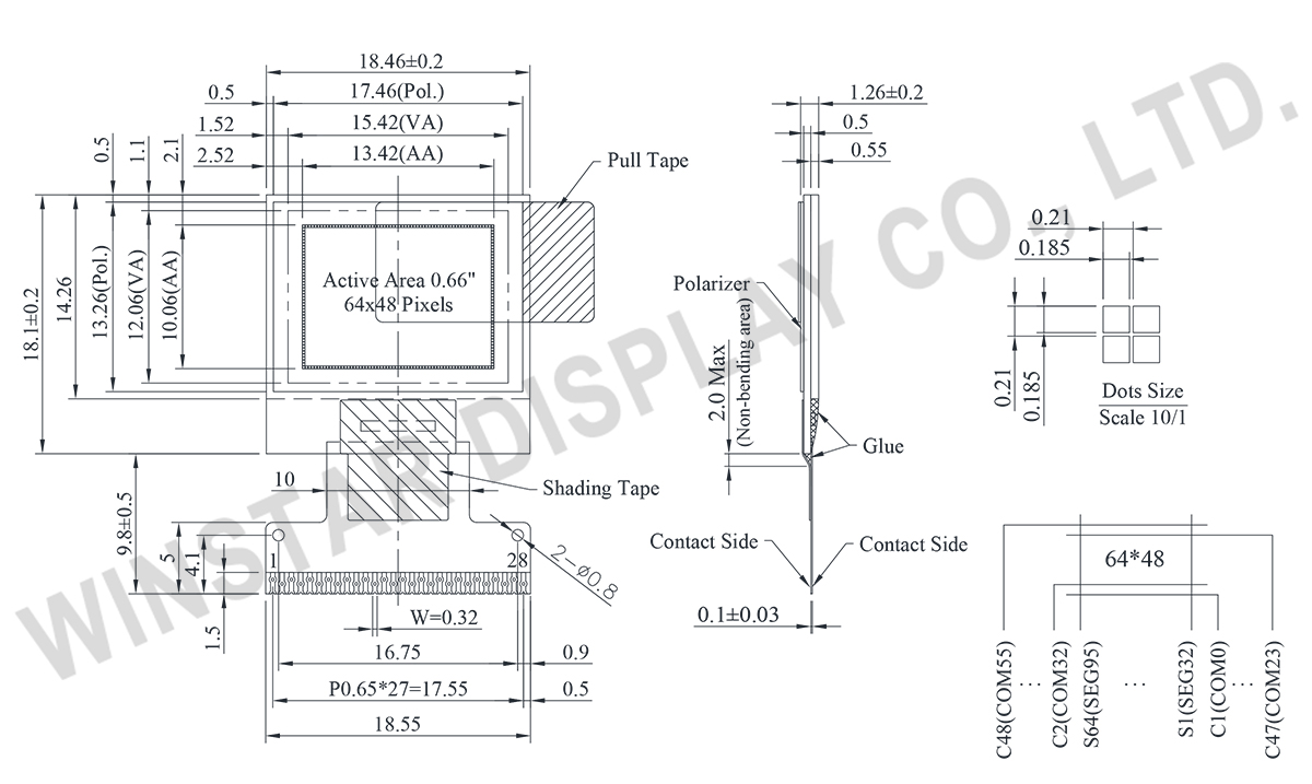
规格图
Data source ref:WEO006448BWPP3N0Y000
产品规格
Pin功能定义
| No. | 符号 | 功能说明 | |||||||||||||||
|---|---|---|---|---|---|---|---|---|---|---|---|---|---|---|---|---|---|
| 1 | ESD_GND | It should be connected to ground. | |||||||||||||||
| 2 | C2N | C1P/C1N – Pin for charge pump capacitor; Connect to each other with a capacitor. C2P/C2N – Pin for charge pump capacitor; Connect to each other with a capacitor. |
|||||||||||||||
| 3 | C2P | ||||||||||||||||
| 4 | C1P | ||||||||||||||||
| 5 | C1N | ||||||||||||||||
| 6 | VBAT | Power supply for charge pump regulator circuit.
|
|||||||||||||||
| 7 | VSS | This is a ground pin. | |||||||||||||||
| 8 | VDD | Power supply pin for core logic operation. | |||||||||||||||
| 9 | BS1 | These pins are MCU interface selection input. See the following table.
|
|||||||||||||||
| 10 | BS2 | ||||||||||||||||
| 11 | CS# | The chip is enabled for MCU communication only when CS# is pulled LOW (active LOW). | |||||||||||||||
| 12 | RES# | This pin is reset signal input. When the pin is low, initialization of the chip is executed. Keep this pin HIGH (i.e. connect to VDD) during normal operation. | |||||||||||||||
| 13 | D/C# | This pin is Data/Command control pin connecting to the MCU. When the pin is pulled HIGH, the data at D[7:0] will be interpreted as data. When the pin is pulled LOW, the data at D[7:0] will be transferred. |
|||||||||||||||
| 14 | R/W# | This is read / write control input pin connecting to the MCU interface. When interfacing to a 6800-series microprocessor, this pin will be used as Read/Write (R/W#) selection input. Read mode will be carried out when this pin is pulled HIGH (i.e. connect to VDD) and write mode when LOW. When 8080 interface mode is selected, this pin will be the Write (WR#) input. Data write operation is initiated when this pin is pulled LOW and the chip is selected. When serial or I2C interface is selected, this pin must be connected to VSS. |
|||||||||||||||
| 15 | E/RD# | This pin is MCU interface input. When 6800 interface mode is selected, this pin will be used as the Enable (E) signal. Read/write operation is initiated when this pin is pulled HIGH and the chip is selected. When 8080 interface mode is selected, this pin receives the Read (RD#) signal. Read operation is initiated when this pin is pulled LOW and the chip is selected. When serial or I2C interface is selected, this pin must be connected to VSS |
|||||||||||||||
| 16~23 | D0~D7 | These are 8-bit bi-directional data bus to be connected to the microprocessor’s data bus. When serial interface mode is selected, D0 will be the serial clock input: SCLK; D1 will be the serial data input: SDIN. When I2C mode is selected, D2, D1 should be tied together and serve as SDAout, SDAin in application and D0 is the serial clock input, SCL . | |||||||||||||||
| 24 | IREF | This is segment output current reference pin. When external IREF is used, a resistor should be connected between this pin and VSS to maintain the IREF current at 30uA. When internal IREF is used, this pin should be kept NC. |
|||||||||||||||
| 25 | VCOMH | COM signal deselected voltage level. A capacitor should be connected between this pin and VSS. |
|||||||||||||||
| 26 | VCC | Power supply for panel driving voltage. This is also the most positive power voltage supply pin When charge pump is enabled, a capacitor should be connected between this pin and VSS. |
|||||||||||||||
| 27 | VLSS | This is an analog ground pin. It should be connected to VSS externally. | |||||||||||||||
| 28 | ESD GND | It should be connected to ground. |
规格说明
| 项目 | 尺寸 | 单位 |
|---|---|---|
| 点阵(分辨率 | 64 x 48 Dots | - |
| 模块尺寸 | 18.46 × 18.10 × 1.26 | mm |
| 有效区域 | 13.42 × 10.06 | mm |
| 像素大小 | 0.185 × 0.185 | mm |
| 像素间距 | 0.210 × 0.210 | mm |
| 显示模式 | Passive Matrix | |
| 显示颜色 | Monochrome | |
| 驱动方式 | 1/48 Duty | |
| IC | SSD1315 | |
| 接口 | 6800, 8080, 4-Wire SPI, I2C | |
| 尺寸 | 0.66 inch | |
最大绝对额定值
| 参数 | 符号 | 最小值 | 最大值 | 单位 |
|---|---|---|---|---|
| 电源电压 | VDD | 0 | 4.0 | V |
| 电荷帮浦稳压器电源电压 | VBAT | 0 | 6.0 | V |
| 显示电源电压 | VCC | 0 | 18.0 | V |
| 工作温度 | TOP | -30 | +70 | °C |
| 储存温度 | TSTG | -30 | +70 | °C |
电气特性
| 项目 | 符号 | 条件 | 最小值 | 典型值 | 最大值 | 单位 |
|---|---|---|---|---|---|---|
| 逻辑电源电压 | VDD | - | 1.65 | 3.0 | 3.3 | V |
| 显示电源电压(外部提供) | VCC | - | 6.0 | 7.5 | 15.0 | V |
| 电荷帮浦稳压器电源电压 | VBAT | - | 3.0 | 3.3 | VDD | V |
| 用于显示的电荷泵输出电压(由内部 DC/DC 生成) | - | 7.0 | 7.5 | 0.2×VDD | V | |
| 输入高电压 | VIH | - | 0.8×VDD | - | VDD | V |
| 输入低电压 | VIL | - | 0 | - | 0.1×VDD | V |
| 输出高电压 | VOH | - | 0.9×VDD | - | 30 | V |
| 输出低电压 | VOL | - | 0 | - | 30 | V |
| 显示 50% 像素(外部提供 VCC) | ICC | VCC=7.5V | - | 3 | 30 | mA |
| 在(由内部 DC/DC 生成的 VCC)上显示 50% 像素 | IBAT | - | - | 15 | 30 | mA |
Search keyword: 64x48 oled, oled 64x48, 0.66 oled, 0.66" oled, 0.66 寸 oled, oled 0.66, oled 0.66", I2C oled display, SPI oled, mini oled
