


설명
도면
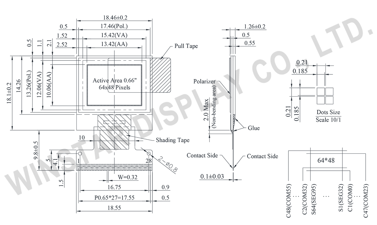
Data source ref:WEO006448BWPP3N0Y000
사양
인터페이스 핀 기능
| No. | 기호 | 기능 | |||||||||||||||
|---|---|---|---|---|---|---|---|---|---|---|---|---|---|---|---|---|---|
| 1 | ESD_GND | It should be connected to ground. | |||||||||||||||
| 2 | C2N | C1P/C1N – Pin for charge pump capacitor; Connect to each other with a capacitor. C2P/C2N – Pin for charge pump capacitor; Connect to each other with a capacitor. |
|||||||||||||||
| 3 | C2P | ||||||||||||||||
| 4 | C1P | ||||||||||||||||
| 5 | C1N | ||||||||||||||||
| 6 | VBAT | Power supply for charge pump regulator circuit.
|
|||||||||||||||
| 7 | VSS | This is a ground pin. | |||||||||||||||
| 8 | VDD | Power supply pin for core logic operation. | |||||||||||||||
| 9 | BS1 | These pins are MCU interface selection input. See the following table.
|
|||||||||||||||
| 10 | BS2 | ||||||||||||||||
| 11 | CS# | The chip is enabled for MCU communication only when CS# is pulled LOW (active LOW). | |||||||||||||||
| 12 | RES# | This pin is reset signal input. When the pin is low, initialization of the chip is executed. Keep this pin HIGH (i.e. connect to VDD) during normal operation. | |||||||||||||||
| 13 | D/C# | This pin is Data/Command control pin connecting to the MCU. When the pin is pulled HIGH, the data at D[7:0] will be interpreted as data. When the pin is pulled LOW, the data at D[7:0] will be transferred. |
|||||||||||||||
| 14 | R/W# | This is read / write control input pin connecting to the MCU interface. When interfacing to a 6800-series microprocessor, this pin will be used as Read/Write (R/W#) selection input. Read mode will be carried out when this pin is pulled HIGH (i.e. connect to VDD) and write mode when LOW. When 8080 interface mode is selected, this pin will be the Write (WR#) input. Data write operation is initiated when this pin is pulled LOW and the chip is selected. When serial or I2C interface is selected, this pin must be connected to VSS. |
|||||||||||||||
| 15 | E/RD# | This pin is MCU interface input. When 6800 interface mode is selected, this pin will be used as the Enable (E) signal. Read/write operation is initiated when this pin is pulled HIGH and the chip is selected. When 8080 interface mode is selected, this pin receives the Read (RD#) signal. Read operation is initiated when this pin is pulled LOW and the chip is selected. When serial or I2C interface is selected, this pin must be connected to VSS |
|||||||||||||||
| 16~23 | D0~D7 | These are 8-bit bi-directional data bus to be connected to the microprocessor’s data bus. When serial interface mode is selected, D0 will be the serial clock input: SCLK; D1 will be the serial data input: SDIN. When I2C mode is selected, D2, D1 should be tied together and serve as SDAout, SDAin in application and D0 is the serial clock input, SCL . | |||||||||||||||
| 24 | IREF | This is segment output current reference pin. When external IREF is used, a resistor should be connected between this pin and VSS to maintain the IREF current at 30uA. When internal IREF is used, this pin should be kept NC. |
|||||||||||||||
| 25 | VCOMH | COM signal deselected voltage level. A capacitor should be connected between this pin and VSS. |
|||||||||||||||
| 26 | VCC | Power supply for panel driving voltage. This is also the most positive power voltage supply pin When charge pump is enabled, a capacitor should be connected between this pin and VSS. |
|||||||||||||||
| 27 | VLSS | This is an analog ground pin. It should be connected to VSS externally. | |||||||||||||||
| 28 | ESD GND | It should be connected to ground. |
기계적 데이터
| 항목 | 치수 | 단위 |
|---|---|---|
| 도트 매트릭스 | 64 x 48 Dots | - |
| 모듈 치수 | 18.46 × 18.10 × 1.26 | mm |
| 활성 영역 | 13.42 × 10.06 | mm |
| 도트 크기 | 0.185 × 0.185 | mm |
| 도트 피치 | 0.210 × 0.210 | mm |
| 디스플레이 모드 | 패시브 매트릭스 (Passive Matrix) | |
| 디스플레이 색 | Monochrome | |
| Drive Duty | 1/48 Duty | |
| IC | SSD1315 | |
| 인터페이스 | 6800, 8080, 4-Wire SPI, I2C | |
| 크기 | 0.66 inch | |
절대 최대 정격값
| Parameter | 기호 | 최소값 | 최대값 | 단위 |
|---|---|---|---|---|
| 전원 전압 | VDD | 0 | 4.0 | V |
| 차지 펌프 레귤레이터 공급 전압 | VBAT | 0 | 6.0 | V |
| 디스플레이 공급 전압 | VCC | 0 | 18.0 | V |
| 작동 온도 | TOP | -30 | +70 | °C |
| 보관 온도 | TSTG | -30 | +70 | °C |
전기적 특성
| 항목 | 기호 | 조건 | 최소값 | 대표값 | 최대값 | 단위 |
|---|---|---|---|---|---|---|
| Supply Voltage for Logic | VDD | - | 1.65 | 3.0 | 3.3 | V |
| Supply Voltage for Display (Supplied Externally) | VCC | - | 6.0 | 7.5 | 15.0 | V |
| Charge Pump Regulator Supply Voltage | VBAT | - | 3.0 | 3.3 | VDD | V |
| Charge Pump Output Voltage for Display (Generated by Internal DC/DC) | Charge Pump VCC | - | 7.0 | 7.5 | 0.2×VDD | V |
| Input High Volt | VIH | - | 0.8×VDD | - | VDD | V |
| Input Low Volt. | VIL | - | 0 | - | 0.1×VDD | V |
| Output High Volt. | VOH | - | 0.9×VDD | - | 30 | V |
| Output Low Volt. | VOL | - | 0 | - | 30 | V |
| 디스플레이 50% 픽셀 켜기(외부에서 VCC 제공) | ICC | VCC=7.5V | - | 3 | 30 | mA |
| 디스플레이 50% 픽셀 켜기(내부 DC/DC에 의해 생성된 VCC) | IBAT | - | - | 15 | 30 | mA |
Search keyword: 64x48 oled, oled 64x48, 0.66 oled, 0.66" oled, 0.66 인치 oled, oled 0.66, oled 0.66", I2C oled display, SPI oled, mini oled
