
- WEO012864U")
 + 프레임으로 - WEF012864U")
우리는 귀하의 프라이버시를 소중히 여깁니다
"모든 쿠키 허용"을 클릭하면 사이트 탐색을 개선하고, 사이트 사용을 분석하며, 마케팅 및 성능 노력에 도움을 주기 위해 쿠키를 귀하의 장치에 저장하는 데 동의한 것으로 간주됩니다. 이 주제에 대한 추가 정보는 당사의 정책에서 확인할 수 있습니다. 개인정보 보호정책


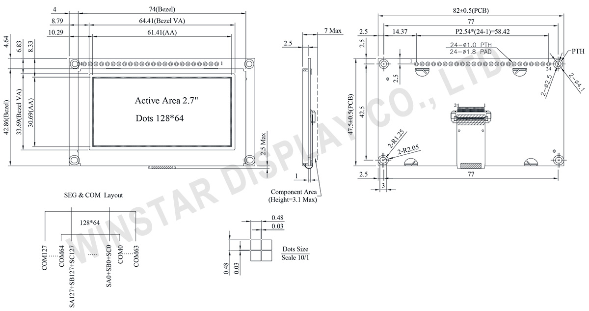
WEP012864U는 COG 구조를 갖춘 128x64 도트의 그래픽 OLED 디스플레이로, 2.7인치 (61.41 × 30.69 mm) 활성 영역을 지원합니다. 이 모듈은 SSD1357 IC를 장착하고 있으며 6800/8080 8비트 및 4와이어 SPI, 그리고 I2C 인터페이스를 지원합니다. 디스플레이는 4비트 그레이스케일을 지원하며 논리 전압은 3V이며 듀티 사이클은 1/64입니다.
WEP012864U OLED 시리즈에는 애플리케이션과 와이어를 통해 쉽게 연결되는 금속 프레임 및 PCB 보드가 함께 제공됩니다. 고객은 별도의 PCB 보드를 개발할 필요가 없으며 인터페이스 설정 및 VCC 회로가 통합되어 사용자 경험을 간소화합니다. PCB에는 모듈을 애플리케이션 제품에 쉽게 설치하기 위한 4개의 나사 구멍이 디자인되어 있습니다.
이 OLED 모듈은 10,000:1의 높은 콘트라스트 비율을 자랑하며 더 생동감 있고 깊은 검정색과 밝은 흰색을 가능하게 합니다. 이로써 향상된 이미지 품질, 더 선명한 디테일 및 향상된 가독성을 얻을 수 있습니다. 모듈은 -40℃에서 80℃의 온도 범위에서 운영되며 -40℃에서 85℃의 저장 온도 범위가 있습니다.
벽/미터 장치, 가정용 응용 프로그램, 금융 POS, 클라우드/IoT 시스템, 지능형 기술 장치, 에너지 시스템, 통신 시스템, 의료 기기 등에 이상적입니다.
또한 WEO012864U 시리즈에는 금속 프레임 및 PCB가없는 유사한 OLED 패널이 있으며 WEF012864U 시리즈에는 금속 프레임이 있지만 PCB가없는 패널도 있습니다. 터치 기능이 필요한 경우 WEP012864U-CTP 시리즈를 고려하십시오.
| 항목 | 치수 | 단위 |
|---|---|---|
| 도트 매트릭스 | 128 x 64 | Dots |
| 모듈 치수 | 82.0 × 47.5 × 7 Max. | mm |
| 활성 영역 | 61.41 × 30.69 | mm |
| 도트 크기 | 0.45 × 0.45 | mm |
| 도트 피치 | 0.48 × 0.48 | mm |
| 디스플레이 모드 | 패시브 매트릭스 | |
| 디스플레이 색상 | Monochrome | |
| Drive Duty | 1/64 Duty | |
| 그레이스케일 | 4 bits | |
| IC | SSD1357 | |
| 인터페이스 | 6800, 8080, SPI, I2C | |
| 크기 | 2.7 인치 | |
| Parameter | 기호 | 최소값 | 최대값 | 단위 |
|---|---|---|---|---|
| Supply Voltage for Logic | VDD | -0.3 | 4.0 | V |
| 작동 온도 | TOP | -40 | 80 | °C |
| 보관 온도 | TSTG | -40 | 85 | °C |
| 항목 | 기호 | 조건 | 최소값 | 대표값 | 최대값 | 단위 |
|---|---|---|---|---|---|---|
| Supply Voltage for Logic | VDD | - | 2.8 | 3.0 | 3.3 | V |
| High Level Input | VIH | - | 0.8×VDD | - | - | V |
| Low Level Input | VIL | - | - | - | 0.2×VDD | V |
| High Level Output | VOH | - | 0.9×VDD | - | - | V |
| Low Level Output | VOL | - | - | - | 0.1×VDD | V |
| Display 50% Pixel on | IDD | VDD =3V | - | 120 | 180 | mA |
| No. | 기호 | 기능 | |||||||||||||||
|---|---|---|---|---|---|---|---|---|---|---|---|---|---|---|---|---|---|
| 1 | VSS | This is a ground pin. | |||||||||||||||
| 2 | VDD | Power supply pin for core logic operation | |||||||||||||||
| 3 | NC | Reserved Pin The N.C. pin between function pins is reserved for compatible and flexible design. |
|||||||||||||||
| 4 | D/C# | This pin is Data/Command control pin connecting to the MCU. When the pin is pulled HIGH, the data at D[7:0] will be interpreted as data. When the pin is pulled LOW, the data at D[7:0] will be transferred to a command register. In I2C mode, this pin acts as SA0 for slave address selection. |
|||||||||||||||
| 5 | R/W# (WR#) |
This pin is read / write control input pin connecting to the MCU interface. When 6800 interface mode is selected, this pin will be used as Read/Write (R/W#) selection input. Read mode will be carried out when this pin is pulled HIGH and write mode when LOW. When 8080 interface mode is selected, this pin will be the Write (WR#) input. Data write operation is initiated when this pin is pulled LOW and the chip is selected. When serial or I2C interface is selected, this pin must be connected to VSS. |
|||||||||||||||
| 6 | E/RD# | This pin is MCU interface input. When 6800 interface mode is selected, this pin will be used as the Enable (E) signal. Read/write operation is initiated when this pin is pulled HIGH and the chip is selected. When 8080 interface mode is selected, this pin receives the Read (RD#) signal. Read operation is initiated when this pin is pulled LOW and the chip is selected. When serial or I2C interface is selected, this pin must be connected to VSS. |
|||||||||||||||
| 7 | DB0 | These pins are bi-directional data bus connecting to the MCU data bus. Unused pins are recommended to tie LOW. When serial interface mode is selected, D0 will be the serial clock input: SCLK; D1 will be the serial data input: SDIN. When I2C mode is selected, D2, D1 should be tied together and serve as SDAout, SDAin in application and D0 is the serial clock input, SCL. |
|||||||||||||||
| 8 | DB1 | ||||||||||||||||
| 9 | DB2 | ||||||||||||||||
| 10 | DB3 | ||||||||||||||||
| 11 | DB4 | ||||||||||||||||
| 12 | DB5 | ||||||||||||||||
| 13 | DB6 | ||||||||||||||||
| 14 | DB7 | ||||||||||||||||
15 |
NC | No connection. | |||||||||||||||
| 16 | RES# | This pin is reset signal input. When the pin is pulled LOW, initialization of the chip is executed. Keep this pin pull HIGH during normal operation. |
|||||||||||||||
17 |
CS# | Chip Select This pin is the chip select input. The chip is enabled for MCU communication only when CS# is pulled low. |
|||||||||||||||
| 18 | NC | No connection. | |||||||||||||||
| 19 | BS2 | Communicating Protocol Select. These pins are MCU interface selection input. See the following table:
|
|||||||||||||||
| 20 | BS1 | ||||||||||||||||
| 21 | NC | No connection. | |||||||||||||||
| 22 | NC | No connection. | |||||||||||||||
| 23 | NC | No connection. | |||||||||||||||
| 24 | NC | No connection. | |||||||||||||||

"모든 쿠키 허용"을 클릭하면 사이트 탐색을 개선하고, 사이트 사용을 분석하며, 마케팅 및 성능 노력에 도움을 주기 위해 쿠키를 귀하의 장치에 저장하는 데 동의한 것으로 간주됩니다. 이 주제에 대한 추가 정보는 당사의 정책에서 확인할 수 있습니다. 개인정보 보호정책