


도면
Data source ref: WEA012832PLAP3N00000
사양
인터페이스 핀 기능
| No. | 기호 | 기능 |
|---|---|---|
| 1 | GND | Ground. |
| 2 | VCC | Power supply pin for logic. |
| 3 | D0 | When the serial interface is selected, then D0 serves as the serial clock input pad (SCL) and D1 serves as the serial data input pad (SI). |
| 4 | D1 | |
| 5 | RES# | This pin is reset signal input. When the pin is pulled LOW, initialization of the chip is executed. Keep this pin HIGH (i.e. connect to VDD) during normal operation. |
| 6 | D/C# | This is the Data/Command control pad that determines whether the data bits are data or a command. D/C = "H": the inputs at D0 and D1 are treated as display data. D/C = "L": the inputs at D0 and D1 are transferred to the command registers. |
| 7 | CS# | This pin is the chip select input. (active LOW) |
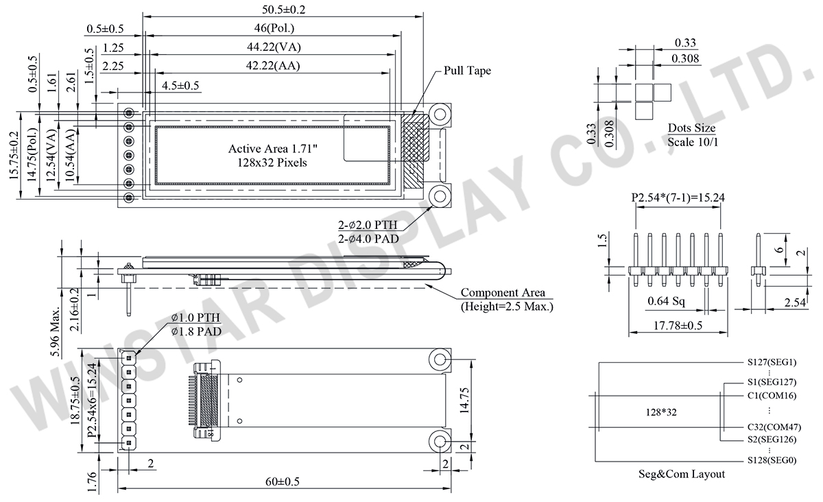
기계적 데이터
| 항목 | 치수 | 단위 |
|---|---|---|
| 도트 매트릭스 | 128 x 32 | - |
| 모듈 치수 | 60.0 × 18.75 × 5.96(MAX) | mm |
| 활성 영역 | 42.22 × 10.54 | mm |
| 도트 크기 | 0.308 × 0.308 | mm |
| 도트 피치 | 0.33 × 0.33 | mm |
| 디스플레이 모드 | 패시브 매트릭스 | |
| 디스플레이 색상 | Monochrome | |
| Drive Duty | 1/32 Duty | |
| IC | CH1115 | |
| 인터페이스 | 4-Wire SPI | |
| 크기 | 1.71 인치 | |
절대 최대 정격값
| Parameter | 기호 | 최소값 | 최대값 | 단위 |
|---|---|---|---|---|
| Supply Voltage for Logic | VCC | -0.3 | 3.6 | V |
| 작동 온도 | TOP | -40 | +80 | °C |
| 보관 온도 | TSTG | -40 | +85 | °C |
전기적 특성
DC 전기적 특성
| 항목 | 기호 | 조건 | 최소값 | 대표값 | 최대값 | 단위 |
|---|---|---|---|---|---|---|
| Supply Voltage for Logic | VCC | - | 1.8 | 3.0 | 3.3 | V |
| High Level Input | VIH | - | 0.8×VCC | - | VCC | V |
| Low Level Input | VIL | - | GND | - | 0.2×VCC | V |
| High Level Output | VOH | - | 0.8×VCC | - | VCC | V |
| Low Level Output | VOL | - | GND | - | 0.2×VCC | V |
| Display 50% Pixel on | ICC | VCC =3V | - | 40 | 30 | mA |
