ピン功能定義
LCM PIN 定義
| Pin |
記号 |
功能定義 |
Remark |
| 1-4 |
NC |
No connection |
|
| 5 |
GND |
Power Ground |
|
| 6 |
NC |
No connection |
|
| 7 |
VCC |
Power voltage |
|
| 8 |
MODE |
Input timing mode selection.
| MODE |
Function |
Note |
| 0 |
DE only |
- |
| 1 |
HS+VS |
Default |
|
|
| 9 |
DE |
Data enable signal for TTL mode. |
|
| 10 |
VS |
Vertical sync input |
|
| 11 |
HS |
Horizontal sync input |
|
| 12 |
B7 |
Blue data(MSB) |
|
| 13 |
B6 |
Blue data |
|
| 14 |
B5 |
Blue data |
|
| 15 |
B4 |
Blue data |
|
| 16 |
B3 |
Blue data |
|
| 17 |
B2 |
Blue data |
|
| 18 |
B1 |
Blue data |
|
| 19 |
B0 |
Blue data(LSB) |
|
| 20 |
G7 |
Green data(MSB) |
|
| 21 |
G6 |
Green data |
|
| 22 |
G5 |
Green data |
|
| 23 |
G4 |
Green data |
|
| 24 |
G3 |
Green data |
|
| 25 |
G2 |
Green data |
|
| 26 |
G1 |
Green data |
|
| 27 |
G0 |
Green data(LSB) |
|
| 28 |
R7 |
Red data(MSB) |
|
| 29 |
R6 |
Red data |
|
| 30 |
R5 |
Red data |
|
| 31 |
R4 |
Red data |
|
| 32 |
R3 |
Red data |
|
| 33 |
R2 |
Red data |
|
| 34 |
R1 |
Red data |
|
| 35 |
R0 |
Red data (LSB) |
|
| 36 |
GND |
Power Ground |
|
| 37 |
DCLK |
Sample clock |
|
| 38 |
GND |
Power Ground |
|
| 39 |
L/R |
Horizontal shift direction (source output) selection.
| L/R |
Source output sequence and data order |
Note |
| 1 |
Left to right |
Default |
| 0 |
Right to left |
- |
|
Note1 |
| 40 |
U/D |
Vertical shift direction (gate output) selection.
| U/D |
Function |
Note |
| 1 |
Top→bottom |
Default |
| 0 |
Bottom→top |
- |
|
Note2 |
| 41 |
NC |
No connection |
|
| 42 |
NC |
No connection |
|
| 43 |
NC |
No connection |
|
| 44 |
RESET |
Reset pin. The chip is in reset state when RESETB=0. |
|
| 45 |
NC |
No connection |
|
| 46 |
NC |
No connection |
|
| 47 |
DITHB |
STBYB Standby mode setting pin. The chip is in standby mode when STBYB=0. |
|
| 48 |
GND |
Power Ground |
|
| 49 |
NC |
No connection |
|
| 50 |
NC |
No connection |
|
Note 1: Selection of scanning mode
| Setting of scan control input |
Scanning direction |
| U/D |
L/R |
| 1 |
1 |
Top to Bottom, left to right |
| 1 |
0 |
Top to Bottom, right to left |
| 0 |
0 |
Bottom to Top, right to left |
| 0 |
1 |
Bottom to Top, left to right |
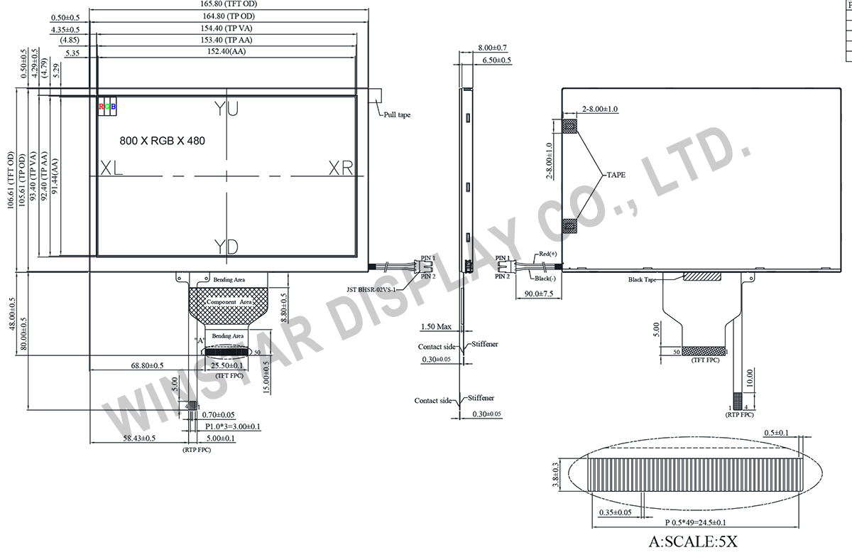
Note 2: Definition of scanning direction.
Refer to the figure as below:
Backlight PIN Definition
| Pin |
記号 |
功能定義 |
| 1 |
VLED+ |
Red, LED_ Anode |
| 2 |
VLED- |
Black, LED_ Cathode |
規格説明
| 項目 |
仕様 |
単位 |
| サイズ (対角線) |
7.0 |
インチ |
| ドットマトリックス(解像度) |
800 x RGB x 480(TFT) |
dots |
| モジュールサイズ |
165.8 (W) x 106.61 (H) x 8.0(D) |
mm |
| 有効エリア |
152.40 x 91.44 |
mm |
| ドットピッチ |
0.1905 x 0.1905 |
mm |
| LCDタイプ |
TFT, 黒色, 透過型 |
| 視野角度 |
80/80/80/80 |
| TFT インターフェイス |
24-bit RGB |
| TFT ドライバIC |
HX8249-A + HX8678-C 或いは互換性IC |
| 画面アスペクト比 |
15:9 |
| バックライトタイプ |
LED・ノーマリ・ホワイト |
| 抵抗膜式タッチパネル |
抵抗式タッチパネル (RTP) |
| 表面処理 |
防眩 |
絶対最大定格
| 項目 |
記号 |
最小値 |
典型値 |
最大値 |
単位 |
| 操作温度 |
TOP |
-30 |
- |
+80 |
℃ |
| 保存温度 |
TST |
-30 |
- |
+80 |
℃ |
電気特性
作業条件
| 項目 |
記号 |
最小値 |
典型値 |
最大値 |
単位 |
| 電源電圧 |
Vcc |
2.7 |
3.3 |
3.6 |
V |
| 電源電流 |
Icc |
- |
101 |
150 |
mA |